
You are looking for information, articles, knowledge about the topic nail salons open on sunday near me smt pcb & nepcon korea 2019 on Google, you do not find the information you need! Here are the best content compiled and compiled by the https://chewathai27.com/to team, along with other related topics such as: smt pcb & nepcon korea 2019 SMD VS SMT, SMD smt, Pcb smt, Surface mount technology, SMT process, SMT machine, SMT assembly, Cách vận hành máy SMT
Surface-mount technology – Wikipedia
- Article author: en.wikipedia.org
- Reviews from users: 27111
 Ratings
 - Top rated: 3.7
- Lowest rated: 1
- Summary of article content: Articles about Surface-mount technology – Wikipedia Updating …
- Most searched keywords: Whether you are looking for Surface-mount technology – Wikipedia Updating
- Table of Contents:
Contents
History[edit]
Common abbreviations[edit]
Assembly techniques[edit]
Advantages[edit]
Disadvantages[edit]
Rework[edit]
Packages[edit]
Identification[edit]
See also[edit]
References[edit]
Navigation menu
SMT là gì? Tất tần tật về công nghệ SMT | HacoLED
- Article author: hacoled.com
- Reviews from users: 45154 Ratings
- Top rated: 3.9
- Lowest rated: 1
- Summary of article content: Articles about SMT là gì? Tất tần tật về công nghệ SMT | HacoLED Updating …
- Most searched keywords: Whether you are looking for SMT là gì? Tất tần tật về công nghệ SMT | HacoLED Updating Hầu hết các thành phần của điện thoại trong túi của bạn – cho dù đó là iPhone 11 hay linh kiện lắp đặt màn hình LED như card màn hình LED được tạo ra thông qua công nghệ gắn kết bề mặt (SMT). Vậy SMT là gì, và tại sao cần phải tạo ra công nghệ này?
- Table of Contents:
SMT là gì
Ưu nhược điểm của công nghệ SMT
Quy trình chung của công nghệ SMT
Sự khác biệt giữa SMT và SMD là gì
Các thành phần SMT chung
Ứng dụng công nghệ SMT
Surface Mount (SMT) PCB Assembly Manufacturer- JLCPCB
- Article author: jlcpcb.com
- Reviews from users: 38536 Ratings
- Top rated: 4.2
- Lowest rated: 1
- Summary of article content: Articles about Surface Mount (SMT) PCB Assembly Manufacturer- JLCPCB Updating …
- Most searched keywords: Whether you are looking for Surface Mount (SMT) PCB Assembly Manufacturer- JLCPCB Updating Have Your PCB Assembled in 24 Hours with In-stock 350k+ Original Components JLCPCB provided. Reduce Your Time And Cost From PCB to PCB assembly ServiceSMT assembly, PCB assembly, PCB SMT assembly, component sourcing, PCB assembly manufacturing
- Table of Contents:
Gia công PCB và PCBA với công nghệ SMT tiên tiến
- Article author: www.thegioiic.com
- Reviews from users: 20711 Ratings
- Top rated: 3.7
- Lowest rated: 1
- Summary of article content: Articles about Gia công PCB và PCBA với công nghệ SMT tiên tiến Updating …
- Most searched keywords: Whether you are looking for Gia công PCB và PCBA với công nghệ SMT tiên tiến Updating Thegioiic nhận gia công PCB từ 2-24 lớp (layer) với chất lượng tốt và giá cả hợp lý. Thegioiic sử dụng công nghệ SMT tiên tiến
- Table of Contents:

SURFACE MOUNT PROCESS – Surface Mount Process
- Article author: www.surfacemountprocess.com
- Reviews from users: 43864 Ratings
- Top rated: 4.1
- Lowest rated: 1
- Summary of article content: Articles about SURFACE MOUNT PROCESS – Surface Mount Process Updating …
- Most searched keywords: Whether you are looking for SURFACE MOUNT PROCESS – Surface Mount Process Updating This website has been created primarily to be a technical resource for surface mount process engineers but also for anyone with an interest in surface mount technology (SMT).Surface mount technology, smt, centroid data, XY data, component placement list, pick and place program, component placement data, design for manufacture and assembly, dfm, dfma, gerber data, process improvement, EMS, electronic manufacturing services, C
- Table of Contents:
Introduction to Surface Mount Technology
What are SMD’s
Surface Mount Assembly Process
Machine programming – Gerber CAD to Centroid Placement XY file
Solder Paste Printing
Solder Paste Inspection (SPI)
Component Placement
Pre-Reflow Automated Optical Inspection (AOI)
First Article Inspection (FAI)
Reflow Soldering
Post-Reflow Automated Optical Inspection (AOI)
Through-hole Assembly – Selective Soldering
Process Verification using X-Ray Inspection
An Increase in Efficiency and Productivity
Enter your email address to learn ways to improve your surface mount process

Máy SMT | Dây chuyền SMT | Giải pháp máy SMT tự động
- Article author: tpa-fas.com.vn
- Reviews from users: 17639 Ratings
- Top rated: 3.4
- Lowest rated: 1
- Summary of article content: Articles about Máy SMT | Dây chuyền SMT | Giải pháp máy SMT tự động Updating …
- Most searched keywords: Whether you are looking for Máy SMT | Dây chuyền SMT | Giải pháp máy SMT tự động Updating Cung cấp các giải pháp về Máy SMT công nghệ hiện đại, phù hợp với quy mô của từng doanh nghiệp, đảm bảo phát triển sản xuất thông minh cho các nhà máy ngành điện – điện tử, ô tô, thiết bị điện…Máy SMT, dây chuyền smt, máy gắn linh kiện, máy làm mạch pcb
- Table of Contents:
Máy SMT là gì Các thiết bị và giải pháp trong dây chuyền SMT
Máy SMT là gì
Máy SMT được phân loại như thế nào
Thị trường máy SMT hiện nay
Giá đựng bảng mạch SMT | PCB magazine rack – Quang Minh ist co.,ltd
- Article author: quangminhist.com
- Reviews from users: 42101 Ratings
- Top rated: 3.6
- Lowest rated: 1
- Summary of article content: Articles about Giá đựng bảng mạch SMT | PCB magazine rack – Quang Minh ist co.,ltd Giá đựng bảng mạch SMT | PCB magazine rack tên tiếng Anh là PCB Magazine Rack chất lượng cao – giá rẻ – miễn phí vận chuyển toàn quốc. Nhận báo giá Giá đựng … …
- Most searched keywords: Whether you are looking for Giá đựng bảng mạch SMT | PCB magazine rack – Quang Minh ist co.,ltd Giá đựng bảng mạch SMT | PCB magazine rack tên tiếng Anh là PCB Magazine Rack chất lượng cao – giá rẻ – miễn phí vận chuyển toàn quốc. Nhận báo giá Giá đựng … Giá đựng bảng mạch SMT | PCB magazine rack tên tiếng Anh là PCB Magazine Rack chất lượng cao – giá rẻ – miễn phí vận chuyển toàn quốc. Nhận báo giá Giá đựng bảng mạch SMT | PCB magazine rack tại đây
- Table of Contents:
Danh mục sản phẩm
Tin tức mới cập nhật
1 Giá đựng bảng mạch SMT ( PCB magazine rack) là gì
2 Chức năng của giá đựng bảng mạch PCB magazine rack
3 Vai trò của giá đựng bản mạch PCB magazine rack trong sản xuất SMT
4 Các loại giá để bản PCB magazine rack mạch thông dụng thường được sử dụng
5 Cấu tạo giá đựng bảng mạch PCB magazine rack
Kích thước 355x320x563mm (9)
Kích thước 355x315x580mm (2)
Kích thước 460x400x563mm (3)
Kích thước 535x460x570mm (2)
Kích thước 535x530x570mm (2)
Giá đựng bảng mạch SMT PCB magazine rack GBM5570 535x530x570mm
Giá đựng bản mạch SMT PCB magazine rack GBM1563 355x320x563mm
Giá đựng bảng mạch SMT PCB magazine rack GBM2563 355x320x563mm
Giá đựng bảng mạch SMT PCB magazine rack GBM5563 355x320x563mm
Giá đựng bảng mạch SMT PCB magazine rack GBM0563 355x320x563mm
Giá đựng bảng mạch SMT PCB magazine rack GBM5370 535x460x570mm
Giá đựng bảng mạch PCB magazine rack GBM4663 460x400x563mm
Giá đựng bản mạch PCB magazine rack GBM5580 355x315x580mm
Giá đựng bảng mạch SMT PCB magazine rack GBM3563 355x320x563mm
Giá đựng bảng mạch SMT PCB magazine rack QGA0104 355x320x563mm
Giá đựng bản mạch SMT PCB magazine rack QGA0105 355x320x563 mm
Giá đựng bản mạch SMT PCB magazine rack QGA0102 355x315x580 mm
Giá đựng bản mạch SMT PCB magazine rack QGA0110 355x320x563 mm
Giá đựng bản mạch SMT PCB magazine rack QGA0107 460x400x563 mm
Giá đựng bản mạch SMT PCB magazine rack QGA0109 535x530x570 mm
Giá đựng bản mạch SMT PCB magazine rack QGA0106 460x400x563 mm
Điều hướng bài viết

smt pcb & nepcon korea 2019
- Article author: shopee.vn
- Reviews from users: 28822 Ratings
- Top rated: 3.3
- Lowest rated: 1
- Summary of article content: Articles about smt pcb & nepcon korea 2019 Updating …
- Most searched keywords: Whether you are looking for smt pcb & nepcon korea 2019 Updating
- Table of Contents:
SMT là gì? máy SMT và dây chuyền công nghệ SMT
- Article author: cncvina.com.vn
- Reviews from users: 35192 Ratings
- Top rated: 4.6
- Lowest rated: 1
- Summary of article content: Articles about SMT là gì? máy SMT và dây chuyền công nghệ SMT Updating …
- Most searched keywords: Whether you are looking for SMT là gì? máy SMT và dây chuyền công nghệ SMT Updating Công nghệ SMT trong sản xuất, lắp ráp bảng mạch điện tử với các dây chuyền lắp ráp linh kiện điện tử tự động do CNC-VINA cung cấp tới khách hàng.
- Table of Contents:
Quy trình dây chuyền công nghệ SMT
GIỚI THIỆU
MÁY TỰ ĐỘNG
DÂY CHUYỀN TỰ ĐỘNG HÓA
Tin tức
DMCA

See more articles in the same category here: Chewathai27.com/to/blog.
Surface-mount technology
Method for producing electronic circuits
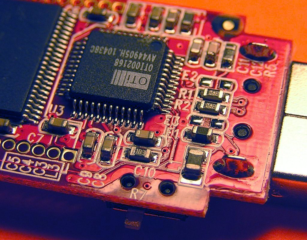
Surface-mount components on a USB flash drive ‘s circuit board. The small rectangular chips with numbers are resistors, while the unmarked small rectangular chips are capacitors. The capacitors and resistors pictured are 0603 (1608 metric) package sizes, along with a very slightly larger 0805 (2012 metric) ferrite bead
MOSFET transistor , placed upon a British postage stamp for size comparison.
Surface-mount technology (SMT) is a method in which the electrical components are mounted directly onto the surface of a printed circuit board (PCB). An electrical component mounted in this manner is referred to as a surface-mount device (SMD). In industry, this approach has largely replaced the through-hole technology construction method of fitting components, in large part because SMT allows for increased manufacturing automation which reduces cost and improves quality. It also allows for more components to fit on a given area of substrate. Both technologies can be used on the same board, with the through-hole technology often used for components not suitable for surface mounting such as large transformers and heat-sinked power semiconductors.
An SMT component is usually smaller than its through-hole counterpart because it has either smaller leads or no leads at all. It may have short pins or leads of various styles, flat contacts, a matrix of solder balls (BGAs), or terminations on the body of the component.
History [ edit ]
Surface mounting was originally called “planar mounting”.[1]
Surface-mount technology was developed in the 1960s. By 1986 surface mounted components accounted for 10% of the market at most, but was rapidly gaining popularity.[2] By the late 1990s, the great majority of high-tech electronic printed circuit assemblies were dominated by surface mount devices. Much of the pioneering work in this technology was done by IBM. The design approach first demonstrated by IBM in 1960 in a small-scale computer was later applied in the Launch Vehicle Digital Computer used in the Instrument Unit that guided all Saturn IB and Saturn V vehicles.[3] Components were mechanically redesigned to have small metal tabs or end caps that could be directly soldered to the surface of the PCB. Components became much smaller and component placement on both sides of a board became far more common with surface mounting than through-hole mounting, allowing much higher circuit densities and smaller circuit boards and, in turn, machines or subassemblies containing the boards.
Often the surface tension of the solder is enough to hold the parts to the board; in rare cases parts on the bottom or “second” side of the board may be secured with a dot of adhesive to keep components from dropping off inside reflow ovens if the part is above the limit of 30g per square inch of pad area.[4] Adhesive is sometimes used to hold SMT components on the bottom side of a board if a wave soldering process is used to solder both SMT and through-hole components simultaneously. Alternatively, SMT and through-hole components can be soldered on the same side of a board without adhesive if the SMT parts are first reflow-soldered, then a selective solder mask is used to prevent the solder holding those parts in place from reflowing and the parts floating away during wave soldering. Surface mounting lends itself well to a high degree of automation, reducing labor cost and greatly increasing production rates.
Conversely, SMT does not lend itself well to manual or low-automation fabrication, which is more economical and faster for one-off prototyping and small-scale production, and this is one reason why many through-hole components are still manufactured. Some SMDs can be soldered with a temperature-controlled manual soldering iron, but unfortunately, those that are very small or have too fine a lead pitch are impossible to manually solder without expensive hot-air solder reflow equipment[dubious – discuss]. SMDs can be one-quarter to one-tenth the size and weight, and one-half to one-quarter the cost of equivalent through-hole parts, but on the other hand, the costs of a certain SMT part and of an equivalent through-hole part may be quite similar, though rarely is the SMT part more expensive.
Common abbreviations [ edit ]
Different terms describe the components, technique, and machines used in manufacturing. These terms are listed in the following table:
SMp term Expanded form SMD Surface-mount devices (active, passive and electromechanical components) SMT Surface-mount technology (assembling and mounting technology) SMA Surface-mount assembly (module assembled with SMT) SMC Surface-mount components (components for SMT) SMP Surface-mount packages (SMD case forms) SME Surface-mount equipment (SMT assembling machines)
Assembly techniques [ edit ]
PCB assembly line: pick-and-place machine followed by an SMT soldering oven
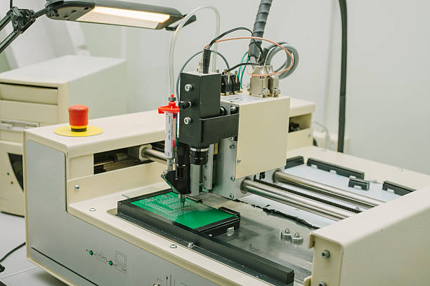
Where components are to be placed, the printed circuit board normally has flat, usually tin-lead, silver, or gold plated copper pads without holes, called solder pads. Solder paste, a sticky mixture of flux and tiny solder particles, is first applied to all the solder pads with a stainless steel or nickel stencil using a screen printing process. It can also be applied by a jet-printing mechanism, similar to an inkjet printer. After pasting, the boards proceed to the pick-and-place machines, where they are placed on a conveyor belt. The components to be placed on the boards are usually delivered to the production line in either paper/plastic tapes wound on reels or plastic tubes. Some large integrated circuits are delivered in static-free trays. Numerical control pick-and-place machines remove the parts from the tapes, tubes or trays and place them on the PCB.[5]
The boards are then conveyed into the reflow soldering oven. They first enter a pre-heat zone, where the temperature of the board and all the components is gradually, uniformly raised to prevent thermal shock. The boards then enter a zone where the temperature is high enough to melt the solder particles in the solder paste, bonding the component leads to the pads on the circuit board. The surface tension of the molten solder helps keep the components in place, and if the solder pad geometries are correctly designed, surface tension automatically aligns the components on their pads.
There are a number of techniques for reflowing solder. One is to use infrared lamps; this is called infrared reflow. Another is to use a hot gas convection. Another technology which is becoming popular again is special fluorocarbon liquids with high boiling points which use a method called vapor phase reflow. Due to environmental concerns, this method was falling out of favor until lead-free legislation was introduced which requires tighter controls on soldering. At the end of 2008, convection soldering was the most popular reflow technology using either standard air or nitrogen gas. Each method has its advantages and disadvantages. With infrared reflow, the board designer must lay the board out so that short components don’t fall into the shadows of tall components. Component location is less restricted if the designer knows that vapor phase reflow or convection soldering will be used in production. Following reflow soldering, certain irregular or heat-sensitive components may be installed and soldered by hand, or in large-scale automation, by focused infrared beam (FIB) or localized convection equipment.
If the circuit board is double-sided then this printing, placement, reflow process may be repeated using either solder paste or glue to hold the components in place. If a wave soldering process is used, then the parts must be glued to the board prior to processing to prevent them from floating off when the solder paste holding them in place is melted.
After soldering, the boards may be washed to remove flux residues and any stray solder balls that could short out closely spaced component leads. Rosin flux is removed with fluorocarbon solvents, high flash point hydrocarbon solvents, or low flash solvents e.g. limonene (derived from orange peels) which require extra rinsing or drying cycles. Water-soluble fluxes are removed with deionized water and detergent, followed by an air blast to quickly remove residual water. However, most electronic assemblies are made using a “No-Clean” process where the flux residues are designed to be left on the circuit board, since they are considered harmless. This saves the cost of cleaning, speeds up the manufacturing process, and reduces waste. However, it is generally suggested to wash the assembly, even when a “No-Clean” process is used, when the application uses very high frequency clock signals (in excess of 1 GHz). Another reason to remove no-clean residues is to improve adhesion of conformal coatings and underfill materials.[6] Regardless of cleaning or not those PCBs, current industry trend suggests to carefully review a PCB assembly process where “No-Clean” is applied, since flux residues trapped under components and RF shields may affect surface insulation resistance (SIR), especially on high component density boards.[7]
Certain manufacturing standards, such as those written by the IPC – Association Connecting Electronics Industries require cleaning regardless of the solder flux type used to ensure a thoroughly clean board. Proper cleaning removes all traces of solder flux, as well as dirt and other contaminants that may be invisible to the naked eye. No-Clean or other soldering processes may leave “white residues” that, according to IPC, are acceptable “provided that these residues have been qualified and documented as benign”.[8] However, while shops conforming to IPC standard are expected to adhere to the Association’s rules on board condition, not all manufacturing facilities apply IPC standard, nor are they required to do so. Additionally, in some applications, such as low-end electronics, such stringent manufacturing methods are excessive both in expense and time required.
Finally, the boards are visually inspected for missing or misaligned components and solder bridging. If needed, they are sent to a rework station where a human operator repairs any errors. They are then usually sent to the testing stations (in-circuit testing and/or functional testing) to verify that they operate correctly.
Automated optical inspection (AOI) systems are commonly used in PCB manufacturing. This technology has proven highly efficient for process improvements and quality achievements.[9]
Advantages [ edit ]
The main advantages of SMT over the older through-hole technique are:
Smaller components.
Much higher component density (components per unit area) and many more connections per component.
Components can be placed on both sides of the circuit board.
Higher density of connections because holes do not block routing space on inner layers, nor on back-side layers if components are mounted on only one side of the PCB.
Small errors in component placement are corrected automatically as the surface tension of molten solder pulls components into alignment with solder pads. (On the other hand, through-hole components cannot be slightly misaligned, because once the leads are through the holes, the components are fully aligned and cannot move laterally out of alignment.)
Better mechanical performance under shock and vibration conditions (partly due to lower mass, and partly due to less cantilevering)
Lower resistance and inductance at the connection; consequently, fewer unwanted RF signal effects and better and more predictable high-frequency performance.
Better EMC performance (lower radiated emissions) due to the smaller radiation loop area (because of the smaller package) and the lesser lead inductance. [10]
Fewer holes need to be drilled. (Drilling PCBs is time-consuming and expensive.)
Lower initial cost and time of setting up for mass production, using automated equipment.
Simpler and faster automated assembly. Some placement machines are capable of placing more than 136,000 components per hour.
Many SMT parts cost less than equivalent through-hole parts.
Disadvantages [ edit ]
SMT may be unsuitable as the sole attachment method for components that are subject to frequent mechanical stress, such as connectors that are used to interface with external devices that are frequently attached and detached. [ citation needed ]
SMDs’ solder connections may be damaged by potting compounds going through thermal cycling.
Manual prototype assembly or component-level repair is more difficult and requires skilled operators and more expensive tools, due to the small sizes and lead spacings of many SMDs. [11] Handling of small SMT components can be difficult, requiring tweezers, unlike nearly all through-hole components. Whereas through-hole components will stay in place (under gravitational force) once inserted and can be mechanically secured prior to soldering by bending out two leads on the solder side of the board, SMDs are easily moved out of place by a touch of a soldering iron. Without developed skill, when manually soldering or desoldering a component, it is easy to accidentally reflow the solder of an adjacent SMT component and unintentionally displace it, something that is almost impossible to do with through-hole components.
Handling of small SMT components can be difficult, requiring tweezers, unlike nearly all through-hole components. Whereas through-hole components will stay in place (under gravitational force) once inserted and can be mechanically secured prior to soldering by bending out two leads on the solder side of the board, SMDs are easily moved out of place by a touch of a soldering iron. Without developed skill, when manually soldering or desoldering a component, it is easy to accidentally reflow the solder of an adjacent SMT component and unintentionally displace it, something that is almost impossible to do with through-hole components. Many types of SMT component packages cannot be installed in sockets, which provide for easy installation or exchange of components to modify a circuit and easy replacement of failed components. (Virtually all through-hole components can be socketed.)
SMDs cannot be used directly with plug-in breadboards (a quick snap-and-play prototyping tool), requiring either a custom PCB for every prototype or the mounting of the SMD upon a pin-leaded carrier. For prototyping around a specific SMD component, a less-expensive breakout board may be used. Additionally, stripboard style protoboards can be used, some of which include pads for standard sized SMD components. For prototyping, “dead bug” breadboarding can be used. [12]
Solder joint dimensions in SMT quickly become much smaller as advances are made toward ultra-fine pitch technology. The reliability of solder joints becomes more of a concern, as less and less solder is allowed for each joint. Voiding is a fault commonly associated with solder joints, especially when reflowing a solder paste in the SMT application. The presence of voids can deteriorate the joint strength and eventually lead to joint failure. [13] [14]
SMDs, usually being smaller than equivalent through-hole components, have less surface area for marking, requiring marked part ID codes or component values to be more cryptic and smaller, often requiring magnification to be read, whereas a larger through-hole component could be read and identified by the unaided eye. This is a disadvantage for prototyping, repair, rework, reverse engineering, and possibly for production set-up.
Rework [ edit ]
Defective surface-mount components can be repaired by using soldering irons (for some connections), or using a non-contact rework system. In most cases a rework system is the better choice because SMD work with a soldering iron requires considerable skill and is not always feasible.
Reworking usually corrects some type of error, either human- or machine-generated, and includes the following steps:
Melt solder and remove component(s)
Remove residual solder
Print solder paste on PCB, directly or by dispensing
Place new component and reflow.
Sometimes hundreds or thousands of the same part need to be repaired. Such errors, if due to assembly, are often caught during the process. However, a whole new level of rework arises when component failure is discovered too late, and perhaps unnoticed until the end user of the device being manufactured experiences it. Rework can also be used if products of sufficient value to justify it require revision or re-engineering, perhaps to change a single firmware-based component. Reworking in large volume requires an operation designed for that purpose.
There are essentially two non-contact soldering/desoldering methods: infrared soldering and soldering with hot gas.[15]
Infrared [ edit ]
With infrared soldering, the energy for heating up the solder joint is transmitted by long- or short-wave infrared electromagnetic radiation.
Advantages:
Easy setup
No compressed air required
No requirement for different nozzles for many component shapes and sizes, reducing cost and the need to change nozzles
Fast reaction of infrared source (depends on system used)
Disadvantages:
Central areas will be heated more than peripheral areas
Temperature control is less precise, and there may be peaks
Nearby components must be shielded from heat to prevent damage, which requires additional time for every board
Surface temperature depends on the component’s albedo: dark surfaces will be heated more than lighter surfaces
The temperature additionally depends on the surface shape. Convective loss of energy will reduce the temperature of the component
No reflow atmosphere possible
Hot gas [ edit ]
During hot gas soldering, the energy for heating up the solder joint is transmitted by a hot gas. This can be air or inert gas (nitrogen).
Advantages:
Simulating reflow oven atmosphere
Some systems allow switching between hot air and nitrogen
Standard and component-specific nozzles allow high reliability and faster processing
Allow reproducible soldering profiles
Efficient heating, large amounts of heat can be transferred
Even heating of the affected board area
Temperature of the component will never exceed the adjusted gas temperature
Rapid cooling after reflow, resulting in small-grained solder joints (depends on system used)
Disadvantages:
Thermal capacity of the heat generator results in slow reaction whereby thermal profiles can be distorted (depends on system used)
Packages [ edit ]
Example of component sizes, metric and imperial codes for two-terminal packages and comparison included
Surface-mount components are usually smaller than their counterparts with leads, and are designed to be handled by machines rather than by humans. The electronics industry has standardized package shapes and sizes (the leading standardisation body is JEDEC).
Identification [ edit ]
Resistors For 5% precision SMD resistors usually are marked with their resistance values using three digits: two significant digits and a multiplier digit. These are quite often white lettering on a black background, but other colored backgrounds and lettering can be used. For 1% precision SMD resistors, the code is used, as three digits would otherwise not convey enough information. This code consists of two digits and a letter: the digits denote the value’s position in the E96 Series of values, while the letter indicates the multiplier.[16] Capacitors Non-electrolytic capacitors are usually unmarked and the only reliable method of determining their value is removal from the circuit and subsequent measurement with a capacitance meter or impedance bridge. The materials used to fabricate the capacitors, such as nickel tantalate, possess different colours and these can give an approximate idea of the capacitance of the component.[ citation needed ] Generally physical size is proportional to capacitance and (squared) voltage for the same dielectric. For example, a 100 nF, 50 V capacitor may come in the same package as a 10 nF, 150 V device. SMD (non-electrolytic) capacitors, which are usually monolithic ceramic capacitors, exhibit the same body color on all four faces not covered by the end caps. SMD electrolytic capacitors, usually tantalum capacitors, and film capacitors are marked like resistors, with two significant figures and a multiplier in units of picofarads or pF, (10−12 farad.) Inductors Smaller inductance with moderately high current ratings are usually of the ferrite bead type. They are simply a metal conductor looped through a ferrite bead and almost the same as their through-hole versions but possess SMD end caps rather than leads. They appear dark grey and are magnetic, unlike capacitors with a similar dark grey appearance. These ferrite bead type are limited to small values in the nanohenry (nH) range and are often used as power supply rail decouplers or in high frequency parts of a circuit. Larger inductors and transformers may of course be through-hole mounted on the same board. SMT inductors with larger inductance values often have turns of wire or flat strap around the body or embedded in clear epoxy, allowing the wire or strap to be seen. Sometimes a ferrite core is present also. These higher inductance types are often limited to small current ratings, although some of the flat strap types can handle a few amps. As with capacitors, component values and identifiers for smaller inductors are not usually marked on the component itself; if not documented or printed on the PCB, measurement, usually removed from the circuit, is the only way of determining them. Larger inductors, especially wire-wound types in larger footprints, usually have the value printed on the top. For example, “330”, which equates to a value of 33 μH. Discrete semiconductors Discrete semiconductors, such as diodes and transistors are often marked with a two- or three-symbol code. The same code marked on different packages or on devices from different manufacturers can translate to different devices. Many of these codes, used because the devices are too small to be marked with more traditional numbers used on larger packages, correlate to more familiar traditional part numbers when a correlation list is consulted. GM4PMK in the United Kingdom has prepared a correlation list, and a similar .pdf list is also available, although these lists are not complete. Integrated circuits Generally, integrated circuit packages are large enough to be imprinted with the complete part number which includes the manufacturer’s specific prefix, or a significant segment of the part number and the manufacturer’s name or logo.
See also [ edit ]
SMT là gì? Tất tần tật về công nghệ SMT
Khi các thiết kế điện tử ngày nay trở nên nhỏ hơn và phức tạp hơn, nhiều kỹ sư đang dựa vào công nghệ dán bề mặt. Sau những năm 1980, công nghệ này đã trở thành công nghệ lắp ráp PCB được ưa chuộng trong sản xuất điện tử và không hề bị loại bỏ kể từ đó.
Hầu hết các thành phần của điện thoại trong túi của bạn – cho dù đó là iPhone 11 hay linh kiện lắp đặt màn hình LED như card màn hình LED được tạo ra thông qua công nghệ gắn kết bề mặt (SMT).
Vậy SMT là gì, và tại sao cần phải tạo ra công nghệ này?
Công nghệ SMT
Bằng cách sử dụng công nghệ này, bạn có thể đạt được các lắp ráp nhỏ hơn với khả năng lặp lại tuyệt vời. Tất cả điều này là do mức độ tự động hóa và độ chính xác cao đi kèm với công nghệ Surface Mount Technology. Nhiều nhà sản xuất hiện đang sử dụng công nghệ này vì nó cho phép họ thiết kế các PCB nhỏ có trọng lượng nhẹ và nhỏ gọn một cách nhanh chóng.
Tốt hơn nữa, đó là một quá trình nhanh hơn nhiều so với công nghệ xuyên lỗ. Công nghệ Surface Mount không đòi hỏi quá nhiều công việc trong quá trình lắp ráp. SMT là một quá trình đơn giản chỉ cần chọn và đặt các thành phần PCB lên bo mạch.
Đọc thêm: PCB là gì? Cấu tạo và ứng dụng thực tiễn như thế nào?
Ưu nhược điểm của công nghệ SMT
Ưu điểm
KHẢ NĂNG CHI TRẢ
Một trong những lý do khiến việc lắp ráp SMT được hình thành là để giảm chi phí sản xuất.
SMT yêu cầu phải khoan ít lỗ hơn rất nhiều trên bảng mạch. Điều này làm giảm đáng kể chi phí xử lý và xử lý.
Cuối cùng, SMT có nhiều khả năng tạo ra khối lượng lớn, cho phép chi phí trên mỗi đơn vị tốt hơn.
HIỆU QUẢ
Một lợi ích khác của lắp ráp SMT là nó sử dụng không gian bảng mạch theo cách hiệu quả hơn nhiều. Nhờ lắp ráp SMT, các kỹ sư hiện có thể biến các thiết bị điện tử phức tạp thành các cụm nhỏ hơn.
Ngoài việc sử dụng hiệu quả hơn không gian trên PCB, lắp ráp SMT nhanh hơn nhiều, cho phép các nhà sản xuất tăng tổng sản lượng. Để đặt điều này trong viễn cảnh, một cái gì đó có thể mất 1-2 giờ để thực hiện, việc lắp ráp SMT chỉ mất 10 – 15 phút.
TÍNH ĐƠN GIẢN
Trong lắp ráp xuyên lỗ, dây dẫn đi qua các lỗ để kết nối các thành phần. Vì các thành phần SMT được hàn ngay trên PCB nên cấu trúc tổng thể ít phức tạp hơn nhiều .
ÍT MẮC LỖI
Việc lắp ráp SMT phụ thuộc rất nhiều vào máy móc chứ không phụ thuộc quá nhiều vào con người. SMT là một quy trình ít bị lỗi vì nó gần như hoàn toàn tự động.
PHÁT RA BỨC XẠ THẤP
Có lẽ, một trong những ưu điểm đáng kể nhất của công nghệ SMT là phát bức xạ thấp. Khi lắp ráp các bộ phận bằng SMT, bạn sẽ gặp phải lượng bức xạ thấp. Do đó, nó có nghĩa là SMT là một phương pháp lắp ráp an toàn hơn một chút so với các phương pháp lắp ráp khác.
Nhược điểm
Như một số các quy trình sản xuất khác, công nghệ SMT có một số nhược điểm.
Điểm lớn nhất là nó đòi hỏi sự chú ý đến chi tiết cao hơn nhiều so với lắp ráp xuyên lỗ. Ngay cả với quy trình phần lớn được tự động hóa, các thông số thiết kế của bạn vẫn phải được đáp ứng để tạo ra sản phẩm cuối cùng chất lượng. Điều này phần lớn rơi vào vai của nhà thiết kế và nhà sản xuất điện tử.
Rắc rối cũng có thể phát sinh khi SMT được sử dụng để đặt các thành phần vào PCB, nó sẽ hoạt động trong các điều kiện liên quan đến:
Ứng suất cơ học
Môi trường áp lực
Căng thẳng nhiệt độ
Vấn đề này có thể được giảm thiểu bằng cách kết hợp SMT với các quy trình xuyên lỗ để có được những lợi ích của cả hai.
Quy trình chung của công nghệ SMT
In hàn dán trên bo mạch
Quá trình đầu tiên liên quan đến việc in keo hàn lên bảng. Ở đây, người sản xuất sử dụng máy in lụa. Bước này nhằm đảm bảo quá trình hàn các thành phần trên tấm đệm diễn ra tốt đẹp.
Gắn các bộ phận
Thứ hai, việc gắn các bộ phận theo sau. Việc gắn các bộ phận liên quan đến việc đặt linh kiện cẩn thận trên một PCB cố định.
Sự rắn chắc
Sau khi đặt các bộ phận, quá trình đông đặc sẽ diễn ra theo sau. Chức năng của đông đặc là làm tan chảy các chất kết dính SMT. Bằng cách này, các nhà sản xuất đảm bảo rằng các thành phần gắn kết bề mặt sẽ dính chính xác trên bo mạch. Lò đóng rắn nằm ở phía sau của máy định vị sẽ thực hiện quá trình đông đặc.
Hàn lại
Sau khi đông đặc, tiếp theo là hàn lại. Mục đích của hàn lại là để đảm bảo rằng chất hàn nóng chảy và mối nối của bo mạch PCB.
Kiểm tra quang học tự động
Bước thứ năm sau khi hàn lại là kiểm tra quang học tự động ( AOI ). Mục đích chính của AOI là kiểm tra cả chất lượng hàn và lắp ráp. Với tính năng Kiểm tra quang học tự động, có thể phát hiện lỗi đủ sớm trước khi phát hành bo mạch ra thị trường. Đó là điều cần thiết trước khi đi vào sản xuất hàng loạt bảng mạch.
Đọc thêm: AOI là gì?
Cắt ván
Sau khi kiểm tra quang học tự động, họ đang cắt bảng sau. Các nhà thiết kế cắt bảng để tạo thành một cá nhân duy nhất. Có một số phương pháp cắt bằng máy được sử dụng ở đây.
Mài bảng
Sau khi cắt ván theo hình dạng yêu cầu, ngay sau đó sẽ tiến hành mài. Nghiền là một trong những quy trình SMT thiết yếu. Vai trò chính của quá trình mài là để đảm bảo quá trình xay ra khỏi gờ. Phay ra khỏi gờ đảm bảo rằng bạn sẽ có một tấm ván mịn. Trong quá trình sản xuất bo mạch, chắc chắn bạn sẽ gặp phải các cạnh thô. Phay đảm bảo mài nhẵn các cạnh thô.
Phay bảng
Sau khi xay xát, sau đó quy trình cuối cùng tiếp theo. Quá trình cuối cùng bao gồm rửa bảng. Làm sạch bo mạch đảm bảo loại bỏ các cặn hàn có hại như chất trợ dung. Bạn có thể làm sạch bo mạch bằng tay hoặc bằng máy. Có những loại máy đặc biệt có thể giúp bạn có được kết quả làm sạch tốt nhất. May mắn thay, bạn có thể làm sạch thủ công nếu bạn không đủ khả năng mua những chiếc máy làm sạch chuyên dụng như vậy.
Sự khác biệt giữa SMT và SMD là gì?
Có một sự khác biệt đáng kể giữa SMT và SMD. Thật không may, nhiều người không hiểu sự khác biệt giữa cái này. Nếu bạn đang ở đây, hãy tự coi mình là người may mắn. Ở đây, bạn sẽ đánh giá cao sự khác biệt giữa SMT và SMD.
Với SMT, SMT (Công nghệ gắn kết bề mặt) là toàn bộ công nghệ liên quan đến việc hàn và gắn các thành phần điện tử trên bảng mạch. Các tính năng điện tử bao gồm tụ điện, điện trở và bóng bán dẫn trên PCB, chưa kể đến một số ít. Mặc dù bạn có thể đặt các miếng thủ công, nhưng hầu hết, các nhà sản xuất sử dụng máy móc đặc biệt. Với máy móc, kết quả chủ yếu là hoàn hảo và chất lượng cao.
Máy SMT đặc biệt, chủ yếu được gọi là máy Pick-and-Place, cẩn thận chọn và đặt tất cả các thành phần và đặt chúng trên bảng mạch. Một lần nữa, bạn có thể thực hiện việc này theo cách thủ công nếu bạn muốn hoặc có kinh nghiệm làm việc đó theo cách thủ công. Tuy nhiên, bạn có thể phải đi chọn và đặt máy theo yêu cầu để có kết quả tốt nhất cho sản phẩm tốt nhất cho kết quả tốt nhất.
Surface Mount Devices (SMD) là các linh kiện được nhà sản xuất gắn trên mạch điện tử để mạch hoạt động. SMT là công nghệ, trong khi SMD là các bộ phận phù hợp với bảng mạch trần. Các thành phần cơ bản phải tìm đường đến bảng bằng quy trình SMT. Hầu hết, các nhà sản xuất sẵn sàng sử dụng máy móc cạnh tranh để gắn và hàn SMD trên một bảng mạch trần.
Trong giai đoạn đầu, việc đặt các thiết bị gắn trên bề mặt chủ yếu được thực hiện bằng tay. Tuy nhiên, với công nghệ được cải tiến, máy chọn và đặt đã đảm nhận vai trò này. Những chiếc máy này hoàn hảo để chọn và đặt tất cả các bộ phận trên bảng mạch. Họ thực hiện công việc nhanh hơn và hiệu quả hơn nhiều so với việc chọn và đặt các thành phần theo cách thủ công.
Các thành phần SMT chung
Có rất nhiều thành phần thiết bị gắn kết bề mặt. Tất cả các thiết bị này hoạt động đồng bộ để tạo thành một mạch hoạt động. Một số thành phần SMD phổ biến nhất mà bạn có trên bo mạch bao gồm:
Thành phần thụ động: SMD thụ động
Hầu hết các thành phần thụ động bao gồm điện cảm, điện dung và thiết bị tổng hợp. Trên bảng mạch, các thành phần SMD thụ động chủ yếu có hình trụ và hình chữ nhật. Khối lượng của các bộ phận này cũng thấp hơn mười lần so với các bộ phận xuyên lỗ.
Bóng bán dẫn và điện trở
Các bóng bán dẫn và điện trở cũng là các thành phần SMD tiêu chuẩn. Nếu bạn quan sát xung quanh, bạn sẽ không bỏ lỡ các điện trở và bóng bán dẫn trên PCB. Điện trở phân chia điện áp, giảm dòng điện và điều chỉnh mức tín hiệu. Ngoài điện trở, bạn cũng sẽ tìm thấy các bóng bán dẫn trên PCB. Các bóng bán dẫn khuếch đại và chuyển đổi công suất điện tử và tín hiệu điện tử trên một bảng mạch in. Một bóng bán dẫn có thể hoạt động như một công tắc và một bộ khuếch đại cùng một lúc. Thời điểm không có dòng điện đến đế, thì dòng điện nhỏ sẽ chạy giữa bộ phát và bộ thu.
Diode
Bạn sẽ luôn tìm thấy diode trên bảng mạch in. Nhưng các chức năng của điốt là gì? Điốt là thiết bị hai đầu cho phép dòng điện lưu thông, nhưng chỉ theo một hướng. Chúng chủ yếu chuyển đổi Dòng điện xoay chiều (AC) thành Dòng điện một chiều (DC).
Mạch tích hợp
Các mạch tích hợp là các chip logic đơn giản. Nếu không có mạch tích hợp, bo mạch sẽ không hoạt động vì chúng giúp truyền tín hiệu và giảm nhiệt độ bo mạch.
(Các thành phần SMD phổ biến: điện trở quảng cáo bóng bán dẫn)
Ứng dụng công nghệ SMT
Công nghệ gắn kết bề mặt được sử dụng rất nhiều trong sản xuất gần như tất cả các vi mạch điện tử ngày nay. Công nghệ Surface Mount có thể sử dụng để gắn hầu hết các thành phần điện trên PCB.
Công nghệ này đóng gói nhiều linh kiện điện tử hơn vào không gian nhỏ hơn trên PCB. SMT là một công nghệ sẽ tiếp tục phát triển trong những năm tới vì nó sẽ không sớm kết thúc. Nếu bạn là một nhà lắp ráp bảng mạch in, thì cách tốt nhất là sử dụng công nghệ này. Mặc dù nó có thể khiến bạn tốn nhiều tiền hơn, nhưng SMT là một trong những công nghệ tốt nhất để sử dụng.
Gia công PCB và PCBA với công nghệ SMT tiên tiến
Thegioiic nhận gia công PCB từ 2-6 lớp (layer) với chất lượng tốt và giá cả hợp lý.
Báo PCB giá online
Sau đây là một có sản phẩm điển hình:
PCB 2 lớp phủ thiếc:
PCB 6 lớp mạ vàng:
Số lớp: 1 tới 6 lớp:
Vật liệu: FR-4, CEM-1, CEM-3, High TG, FR4 Halogen Free, Rogers
Độ dày board: 0.21mm to 7.0mm
Độ dày đồng: 0.5 OZ to 7.0 OZ
Lớp dày đồng trong lỗ: >25.0 um (>1mil)
Kích thước board:
Max. Board Size: 23 × 25 (580mm×900mm)
Min. Drilled Hole Size: 3mil (0.075mm)
Min. Line Width: 3mil (0.075mm)
Min. Line Spacing: 3mil (0.075mm)
Hoàn thiện bề mặt (Surface finishing): HASL / HASL lead free, HAL, mạ thiếc, mạ vàng, mạ bạc…
Màu phủ (Solder Mask): Xanh lá, vàng, đen, trắng, đỏ, xanh dương
Sai số:
Sai số hình dáng: ±0.13 mm
Sai số lỗ: PTH: ±0.076mm NPTH: ±0.05mm
Gia công cắm chip SMT PCBA:
Ngoài ra, Thegioiic còn nhận gia công PCBA bằng công nghệ SMT tiên tiến. Thegioiic có ưu điểm nổi bật sau:
Công nghệ máy SMT của Siemens có thể cắm được các loại IC với kiểu chân BGA và QFP, Chip 0402, linh kiện dạng ống,
Số lượng đặt hàng có thể từ 50-5000 PCBA,
Giá cả hợp lý và chất lượng tốt,
Thời gian giao hàng đúng hẹn.
Báo PCB giá online hoặc gửi email [email protected]
So you have finished reading the smt pcb & nepcon korea 2019 topic article, if you find this article useful, please share it. Thank you very much. See more: SMD VS SMT, SMD smt, Pcb smt, Surface mount technology, SMT process, SMT machine, SMT assembly, Cách vận hành máy SMT