
당신은 주제를 찾고 있습니까 “kicad copper pour – Introduction to KiCad course (Copper Fills)“? 다음 카테고리의 웹사이트 Chewathai27.com/you 에서 귀하의 모든 질문에 답변해 드립니다: Chewathai27.com/you/blog. 바로 아래에서 답을 찾을 수 있습니다. 작성자 Javier Martinez 이(가) 작성한 기사에는 조회수 5,863회 및 좋아요 62개 개의 좋아요가 있습니다.
Table of Contents
kicad copper pour 주제에 대한 동영상 보기
여기에서 이 주제에 대한 비디오를 시청하십시오. 주의 깊게 살펴보고 읽고 있는 내용에 대한 피드백을 제공하세요!
d여기에서 Introduction to KiCad course (Copper Fills) – kicad copper pour 주제에 대한 세부정보를 참조하세요
More info at http://www.embedded-learning.academy/
kicad copper pour 주제에 대한 자세한 내용은 여기를 참조하세요.
Kicad Tutorial: Copper pours / fills – Wayne and Layne
A copper pour or fill refers to an area on a printed circuit board where the original copper is not etched away, and remains in place, usually …
Source: www.wayneandlayne.com
Date Published: 5/19/2021
View: 2096
Copper pour doesn’t fill – Layout – KiCad.info Forums
I have a relatively simple PCB that I’m working on the layout. I have created the edge cut layer (Board outline), have placed most …
Source: forum.kicad.info
Date Published: 1/1/2022
View: 7903
Designing PCBs in Kicad and PcbNew: Adding Copper Fills …
In KiCad, filling an area with copper does not create any connections, so the first step is to finish drawing all the traces as normal. Use the highlight tool …
Source: store.curiousinventor.com
Date Published: 6/21/2021
View: 8082
Copper zones won’t fill – EEVblog
The first time I used a filled zone in KiCad they disappeared… in my case this was because the Cu layer where I was creating the fill was …
Source: www.eevblog.com
Date Published: 2/24/2021
View: 6741
[kicad-users] Creating and Filling Copper Zones in KiCAD
closely where the copper fill ends at the line, there are several places where one has ask – why dn’t it fill here? And why are the ends of the
Source: kicad-users.yahoogroups.narkive.com
Date Published: 4/6/2022
View: 7005
주제와 관련된 이미지 kicad copper pour
주제와 관련된 더 많은 사진을 참조하십시오 Introduction to KiCad course (Copper Fills). 댓글에서 더 많은 관련 이미지를 보거나 필요한 경우 더 많은 관련 기사를 볼 수 있습니다.
주제에 대한 기사 평가 kicad copper pour
- Author: Javier Martinez
- Views: 조회수 5,863회
- Likes: 좋아요 62개
- Date Published: 2017. 12. 24.
- Video Url link: https://www.youtube.com/watch?v=1unpkgVhOyA
What are filled zones in PCB?
A copper pour or fill refers to an area on a printed circuit board where the original copper is not etched away, and remains in place, usually electrically connected to the Ground signal, producing a “Ground Plane”.
How do I use Kicad software?
- Under Windows run kicad.exe. …
- Create a new project: File → New → Project. …
- Let’s begin by creating a schematic. …
- Click on the ‘Page Settings’ icon on the top toolbar. …
- We will now place our first component. …
- Click on the middle of your schematic sheet. …
- Double click on it.
Does Kicad have an autorouter?
The autorouter that was included in Kicad 4 has been removed in Kicad 5. It is likely that a new autorouter will be added in the future. Until then, you can use an external autorouter.
What are fill zones?
A high risk area in pharmaceutical manufacture, for sterile filling.
What are stitching vias?
Via stitching is a technique used to tie together larger copper areas on different layers, in effect creating a strong vertical connection through the board structure, helping maintain a low impedance and short return loops.
How do I get KiCad from Gerber?
In KiCad, open your PCB design file and go to File -> Plot, or find the plot icon on the main interface. This will bring up the plot window. Select an output directory for your Gerber Files and select the following layers and options.
Is copper pour necessary?
The Verdict. Copper pour, via fences, and via stitching are useful tools if used properly, but they could create a new EMI problem if not used properly.
What is the purpose of a copper pour?
In electronics, the term copper pour refers to an area on a printed circuit board filled with copper (the metal used to make connections in printed circuit boards). Copper pour is commonly used to create a ground plane.
What is the use of copper area in PCB?
Copper pour – an area of a PCB layer that is filled with copper. The layer may be the top, bottom or any internal to the PCB stackup and the pour may be used as a ground, reference or to isolate specific components or circuitry from the rest of the elements of the layer.
Is KiCad used in industry?
Most people would say KiCad is only for hobbists and Altium, Orcad, PADS and so on, are for professional use and KiCad can’t be used for professional applications. Most of the people that think this way haven’t even used KiCad for a while with the at least version 5.
Is KiCad any good?
KiCad is a reliable and advanced tool for the creation and maintenance of electronic boards. It does not come with board-size restrictions, and it can house 32 copper layers, 14 technical layers, and four secondary layers.
Which is better KiCad or EAGLE?
KiCAD is better if you are interested in a non-licence type software. It does not have any limitations like limited size of the board and single sheet per project like in the Free Version of Eagle. However, If you are getting started Eagle is a great choice as its easy and has very well structured tutorials around.
How do I add a filled zone in KiCad?
Use the highlight tool to highlight the net for which you will be creating a zone(GND in our case). Select the zone tool and click somewhere to start the outline (this will bring up the zone dialog). Select the NET, layer and pad options, which is how the zone will connect to pads that are part of the net.
What is net in KiCad?
In KiCad, each net is part of exactly one net class. If you do not add a net to a specific class, it will be part of the Default class, which always exists. Nets may be added to net classes from either the schematic or PCB editor, via the Schematic Setup and Board Setup dialogs.
Kicad Tutorial: Copper pours / fills
This is part of a series of short tutorials on advanced topics of using Kicad, the favorite schematic/PCB design software here at Wayne and Layne.
A copper pour or fill refers to an area on a printed circuit board where the original copper is not etched away, and remains in place, usually electrically connected to the Ground signal, producing a “Ground Plane”. This has a number of advantages, including decreasing the amount of etching fluid required during manufacturing, as well as reducing the amount of electrical noise and signal crosstalk experienced by the circuit elements.
It is relatively easy to create a copper fill in Kicad. We usually add fills after having already drawn in the PCB outline in the Edges layer. First, ensure that you have selected one of the copper layers (such as “Front†or “F.Cuâ€). Then, select the “Add Filled Zones†from the toolbar on the right side of the screen.
Next, click in one corner of the PCB outline to start drawing the copper fill.
Once you click in the first corner, the following properties box will appear. Select the relevant copper layer (here, either “F.Cu” or “B.Cu”) and the desired net for the fill (usually you want “GND”, but sometimes you might want some other net, or “
” which will make an isolated copper fill). The settings in the bottom half are important for controlling the drawing of the filled area as well as the “thermals”. One potential problem with adding ground fill is that the ground pads will become very difficult to solder, as the ground plane will suck away all the heat from your soldering iron, and the pad won’t ever heat up hot enough for the solder to flow. To avoid this problem, you almost always want to add “thermal relief” to your ground pads, which means there is a keep-out area adjacent to each ground pad where there is no fill, and instead each ground pad is connected by a number of thinner traces. This still provides a very good electrical connection for the ground pad, but makes it much easier to solder. The “Clearance” setting controls the general clearance between the filled area and pads/traces of other nets. The “Minimum width” setting controls the thinnest that the fill can be when flowing around other pads/traces. The “Thermal Reliefs” settings control the clearance around the ground pads (0.040″ here) and the width of the traces connecting from the fill to the ground pads (0.009″ here). We’ve found these settings to work pretty well for most of our projects. You also want to select “Arbitrary” for the “Outline Slope” setting to make it easier to draw the zone outline. Click “OK” to close this window and continue drawing the fill outline. (Click the image to enlarge) Once you have closed the zone properties window, click once in each of the other three corners (in order) on the board outline. Then, to complete the final segment, double-click on the original corner to end the zone. You should see red or green hatching (depending on which copper layer you used) on the edges of your PCB indicating the filled region, as shown in the image below.
Generally you want to have a copper fill on both the top and bottom of the PCB. To add the fill on the other side, the easiest way is to right-click on the existing board edge, select “Zone outline”, then go to “Zones”->”Duplicate Zone”. This brings up the zone properties box for the new zone, so select the other copper layer and press “OK”.
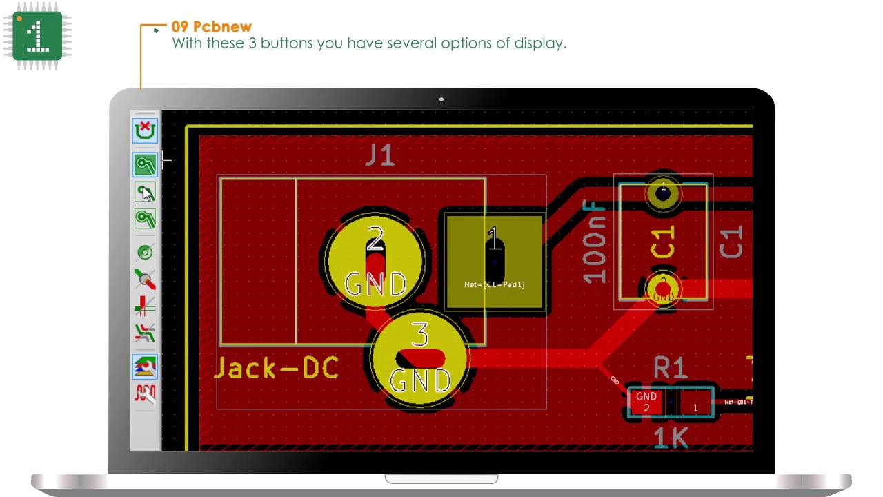
To see the copper fills in your design, click on the “Show filled areas in zones” button, the 10th button in the left-size toolbar. The button below that will hide the fills. Then, you can run the DRC tool (Ladybug Checkmark in the top toolbar) which will fill all your zones. You should see something like the image below. The brown-yellow color is the combination of red (top side) and green (bottom side) copper fills. We can see the 20 mil clearance between the fill and non-ground copper, and the larger 40 mil clearance between the fill and GND pads.
Other tutorials in this series:
Kicad Tutorial: Copper pours / fills
This is part of a series of short tutorials on advanced topics of using Kicad, the favorite schematic/PCB design software here at Wayne and Layne.
A copper pour or fill refers to an area on a printed circuit board where the original copper is not etched away, and remains in place, usually electrically connected to the Ground signal, producing a “Ground Plane”. This has a number of advantages, including decreasing the amount of etching fluid required during manufacturing, as well as reducing the amount of electrical noise and signal crosstalk experienced by the circuit elements.
It is relatively easy to create a copper fill in Kicad. We usually add fills after having already drawn in the PCB outline in the Edges layer. First, ensure that you have selected one of the copper layers (such as “Front†or “F.Cuâ€). Then, select the “Add Filled Zones†from the toolbar on the right side of the screen.
Next, click in one corner of the PCB outline to start drawing the copper fill.
Once you click in the first corner, the following properties box will appear. Select the relevant copper layer (here, either “F.Cu” or “B.Cu”) and the desired net for the fill (usually you want “GND”, but sometimes you might want some other net, or “
” which will make an isolated copper fill). The settings in the bottom half are important for controlling the drawing of the filled area as well as the “thermals”. One potential problem with adding ground fill is that the ground pads will become very difficult to solder, as the ground plane will suck away all the heat from your soldering iron, and the pad won’t ever heat up hot enough for the solder to flow. To avoid this problem, you almost always want to add “thermal relief” to your ground pads, which means there is a keep-out area adjacent to each ground pad where there is no fill, and instead each ground pad is connected by a number of thinner traces. This still provides a very good electrical connection for the ground pad, but makes it much easier to solder. The “Clearance” setting controls the general clearance between the filled area and pads/traces of other nets. The “Minimum width” setting controls the thinnest that the fill can be when flowing around other pads/traces. The “Thermal Reliefs” settings control the clearance around the ground pads (0.040″ here) and the width of the traces connecting from the fill to the ground pads (0.009″ here). We’ve found these settings to work pretty well for most of our projects. You also want to select “Arbitrary” for the “Outline Slope” setting to make it easier to draw the zone outline. Click “OK” to close this window and continue drawing the fill outline. (Click the image to enlarge) Once you have closed the zone properties window, click once in each of the other three corners (in order) on the board outline. Then, to complete the final segment, double-click on the original corner to end the zone. You should see red or green hatching (depending on which copper layer you used) on the edges of your PCB indicating the filled region, as shown in the image below.
Generally you want to have a copper fill on both the top and bottom of the PCB. To add the fill on the other side, the easiest way is to right-click on the existing board edge, select “Zone outline”, then go to “Zones”->”Duplicate Zone”. This brings up the zone properties box for the new zone, so select the other copper layer and press “OK”.
To see the copper fills in your design, click on the “Show filled areas in zones” button, the 10th button in the left-size toolbar. The button below that will hide the fills. Then, you can run the DRC tool (Ladybug Checkmark in the top toolbar) which will fill all your zones. You should see something like the image below. The brown-yellow color is the combination of red (top side) and green (bottom side) copper fills. We can see the 20 mil clearance between the fill and non-ground copper, and the larger 40 mil clearance between the fill and GND pads.
Other tutorials in this series:
Getting Started in KiCad
Under Windows run kicad.exe. Under Linux type ‘kicad’ in your Terminal. You are now in the main window of the KiCad project manager. From here you have access to eight stand-alone software tools: Eeschema, Schematic Library Editor, Pcbnew, PCB Footprint Editor, GerbView, Bitmap2Component, PCB Calculator and Pl Editor. Refer to the work-flow chart to give you an idea how the main tools are used.
Create a new project: File → New → Project. Name the project file ‘tutorial1’. The project file will automatically take the extension “.pro”. The exact appearance of the dialog depends on the used platform, but there should be a checkbox for creating a new directory. Let it stay checked unless you already have a dedicated directory. All your project files will be saved there.
Let’s begin by creating a schematic. Start the schematic editor Eeschema, . It is the first button from the left.
Click on the ‘Page Settings’ icon on the top toolbar. Set the appropriate ‘paper size’ (‘A4′,’8.5×11’ etc.) and enter the Title as ‘Tutorial1’. You will see that more information can be entered here if necessary. Click OK. This information will populate the schematic sheet at the bottom right corner. Use the mouse wheel to zoom in. Save the whole schematic: File → Save
We will now place our first component. Click on the ‘Place symbol’ icon in the right toolbar. You may also press the ‘Add Symbol’ hotkey [a].
Click on the middle of your schematic sheet. A Choose Symbol window will appear on the screen. We’re going to place a resistor. Search / filter on the ‘R’ of Resistor. You may notice the ‘Device’ heading above the Resistor. This ‘Device’ heading is the name of the library where the component is located, which is quite a generic and useful library.
Double click on it. This will close the ‘Choose Symbol’ window. Place the component in the schematic sheet by clicking where you want it to be.
Click on the magnifier icon to zoom in on the component. Alternatively, use the mouse wheel to zoom in and zoom out. Press the wheel (central) mouse button to pan horizontally and vertically.
Try to hover the mouse over the component ‘R’ and press [r]. The component should rotate. You do not need to actually click on the component to rotate it. Sometimes, if your mouse is also over something else, a menu will appear. You will see the Clarify Selection menu often in KiCad; it allows working on objects that are on top of each other. In this case, tell KiCad you want to perform the action on the ‘Symbol …R…’ if the menu appears.
Right click in the middle of the component and select Properties → Edit Value. You can achieve the same result by hovering over the component and pressing [v]. Alternatively, [e] will take you to the more general Properties window. Notice how the right-click menu below shows the hotkeys for all available actions.
The Edit Value Field window will appear. Replace the current value ‘R’ with ‘1 k’. Click OK. Do not change the Reference field (R?), this will be done automatically later on. The value above the resistor should now be ‘1 k’.
To place another resistor, simply click where you want the resistor to appear. The symbol selection window will appear again.
The resistor you previously chose is now in your history list, appearing as ‘R’. Click OK and place the component.
In case you make a mistake and want to delete a component, right click on the component and click ‘Delete’. This will remove the component from the schematic. Alternatively, you can hover over the component you want to delete and press [Delete].
You can also duplicate a component already on your schematic sheet by hovering over it and pressing [c]. Click where you want to place the new duplicated component.
Right click on the second resistor. Select ‘Drag’. Reposition the component and left click to drop. The same functionality can be achieved by hovering over the component and by pressing [g]. [r] will rotate the component while [x] and [y] will flip it about its x- or y-axis. Right-Click → Move or [m] is also a valuable option for moving anything around, but it is better to use this only for component labels and components yet to be connected. We will see later on why this is the case.
Edit the second resistor by hovering over it and pressing [v]. Replace ‘R’ with ‘100’. You can undo any of your editing actions with Ctrl+Z.
Change the grid size. You have probably noticed that on the schematic sheet all components are snapped onto a large pitch grid. You can easily change the size of the grid by Right-Click → Grid. In general, it is recommended to use a grid of 50.0 mils for the schematic sheet.
We are going to add a component from a library that may not be configured in the default project. In the menu, choose Preferences → Manage Symbol Libraries. In the Symbol Libraries window you can see two tabs: Global Libraries and Project Specific Libraries. Each one has one sym-lib-table file. For a library (.lib file) to be available it must be in one of those sym-lib-table files. If you have a library file in your file system and it’s not yet available, you can add it to either one of the sym-lib-table files. For practice we will now add a library which already is available.
Select the Project Specific table. Click the file browser button below the table. You need to find where the official KiCad libraries are installed on your computer. Look for a library directory containing a hundred of .dcm and .lib files. Try in C:\Program Files (x86)\KiCad\share\ (Windows) and /usr/share/kicad/library/ (Linux). When you have found the directory, choose and add the ‘MCU_Microchip_PIC12.lib’ library and close the window. It will be added to the end of of the list. Now click its nickname and change it to ‘microchip_pic12mcu’. Close the Symbol Libraries window with OK.
Repeat the add-component steps, however this time select the ‘microchip_pic12mcu’ library instead of the ‘Device’ library and pick the ‘PIC12C508A-ISN’ component.
Hover the mouse over the microcontroller component. Notice that [x] and [y] again flip the component. Keep the symbol mirrored around the Y axis so that the pins G0 and G1 point to right.
Repeat the add-component steps, this time choosing the ‘Device’ library and picking the ‘LED’ component from it.
Organise all components on your schematic sheet as shown below.
We now need to create the schematic component ‘MYCONN3’ for our 3-pin connector. You can jump to the section titled Make Schematic Symbols in KiCad to learn how to make this component from scratch and then return to this section to continue with the board.
You can now place the freshly made component. Press [a] and pick the ‘MYCONN3’ component in the ‘myLib’ library.
The component identifier ‘J?’ will appear under the ‘MYCONN3’ label. If you want to change its position, right click on ‘J?’ and click on ‘Move Field’ (equivalent to [m]). It might be helpful to zoom in before/while doing this. Reposition ‘J?’ under the component as shown below. Labels can be moved around as many times as you please.
It is time to place the power and ground symbols. Click on the ‘Place power port’ button on the right toolbar. Alternatively, press [p]. In the component selection window, scroll down and select ‘VCC’ from the ‘power’ library. Click OK.
Click above the pin of the 1 k resistor to place the VCC part. Click on the area above the microcontroller ‘VDD’. In the ‘Component Selection history’ section select ‘VCC’ and place it next to the VDD pin. Repeat the add process again and place a VCC part above the VCC pin of ‘MYCONN3’. Move references and values out of the way if needed.
Repeat the add-pin steps but this time select the GND part. Place a GND part under the GND pin of ‘MYCONN3’. Place another GND symbol on the left of the VSS pin of the microcontroller. Your schematic should now look something like this:
Next, we will wire all our components. Click on the ‘Place wire’ icon on the right toolbar. Be careful not to pick ‘Place bus’, which appears directly beneath this button but has thicker lines. The section Bus Connections in KiCad will explain how to use a bus section.
Click on the little circle at the end of pin 7 of the microcontroller and then click on the little circle on pin 1 of the LED. Click once when you are drawing the wire to create a corner. You can zoom in while you are placing the connection. If you want to reposition wired components, it is important to use [g] (to grab) and not [m] (to move). Using grab will keep the wires connected. Review step 24 in case you have forgotten how to move a component.
Repeat this process and wire up all the other components as shown below. To terminate a wire just double-click. When wiring up the VCC and GND symbols, the wire should touch the bottom of the VCC symbol and the middle top of the GND symbol. See the screenshot below.
We will now consider an alternative way of making a connection using labels. Pick a net labelling tool by clicking on the ‘Place net label’ icon on the right toolbar. You can also use [l].
Click in the middle of the wire connected to pin 6 of the microcontroller. Name this label ‘INPUT’. The label is still an independent item which you can for example move, rotate and delete. The small anchor rectangle of the label must be exactly on a wire or a pin for the label to take effect.
Follow the same procedure and place another label on line on the right of the 100 ohm resistor. Also name it ‘INPUT’. The two labels, having the same name, create an invisible connection between pin 6 of the PIC and the 100 ohm resistor. This is a useful technique when connecting wires in a complex design where drawing the lines would make the whole schematic messier. To place a label you do not necessarily need a wire, you can simply attach the label to a pin.
Labels can also be used to simply label wires for informative purposes. Place a label on pin 7 of the PIC. Enter the name ‘uCtoLED’. Name the wire between the resistor and the LED as ‘LEDtoR’. Name the wire between ‘MYCONN3’ and the resistor as ‘INPUTtoR’.
You do not have to label the VCC and GND lines because the labels are implied from the power objects they are connected to.
Below you can see what the final result should look like.
Let’s now deal with unconnected wires. Any pin or wire that is not connected will generate a warning when checked by KiCad. To avoid these warnings you can either instruct the program that the unconnected wires are deliberate or manually flag each unconnected wire or pin as unconnected.
Click on the ‘Place no connection flag’ icon on the right toolbar. Click on pins 2, 3, 4 and 5. An X will appear to signify that the lack of a wire connection is intentional.
Some components have power pins that are invisible. You can make them visible by clicking on the ‘Show hidden pins’ icon on the left toolbar. Hidden power pins get automatically connected if VCC and GND naming is respected. Generally speaking, you should try not to make hidden power pins.
It is now necessary to add a ‘Power Flag’ to indicate to KiCad that power comes in from somewhere. Press [a] and search for ‘PWR_FLAG’ which is in ‘power’ library. Place two of them. Connect them to a GND pin and to VCC as shown below. This will avoid the classic schematic checking warning: Pin connected to some other pins but no pin to drive it.
Sometimes it is good to write comments here and there. To add comments on the schematic use the ‘Place text’ icon on the right toolbar.
All components now need to have unique identifiers. In fact, many of our components are still named ‘R?’ or ‘J?’. Identifier assignation can be done automatically by clicking on the ‘Annotate schematic symbols’ icon on the top toolbar.
In the Annotate Schematic window, select ‘Use the entire schematic’ and click on the ‘Annotate’ button. Click ‘Close’. Notice how all the ‘?’ have been replaced with numbers. Each identifier is now unique. In our example, they have been named ‘R1’, ‘R2’, ‘U1’, ‘D1’ and ‘J1’.
We will now check our schematic for errors. Click on the ‘Perform electrical rules check’ icon on the top toolbar. Click on the ‘Run’ button. A report informing you of any errors or warnings such as disconnected wires is generated. You should have 0 Errors and 0 Warnings. In case of errors or warnings, a small green arrow will appear on the schematic in the position where the error or the warning is located. Check ‘Create ERC file report’ and press the ‘Run’ button again to receive more information about the errors. If you have a warning with “No default editor found, you must choose it”, try setting the path to c:\windows
otepad.exe (windows) or /usr/bin/gedit (Linux).
The schematic is now finished. We can now create a Netlist file to which we will add the footprint of each component. Click on the ‘Generate netlist’ icon on the top toolbar. Click on the ‘Generate Netlist’ button and save under the default file name. Netlist was necessary in previous versions of KiCad. In the recent versions you can ignore it and instead use Tools → Update PCB from Schematic. If you do that you have to assign footprints to symbols first.
After generating the Netlist file, click on the ‘Run Cvpcb’ icon on the top toolbar. If a missing file error window pops up, just ignore it and click OK. There are many more ways to add footprints to symbols. Right click on a symbol → Properties → Edit Footprint
Double click on a symbol, or right click on a symbol → Properties → Edit Properties → Footprint
Tools → Edit Symbol Fields
Check Show footprint previews in symbol chooser in Eeschema’s preferences and select the footprint when you select a new symbol to place
Cvpcb allows you to link all the components in your schematic with footprints in the KiCad library. The pane on the center shows all the components used in your schematic. Here select ‘D1’. In the pane on the right you have all the available footprints, here scroll down to ‘LED_THT:LED-D5.0mm’ and double click on it.
It is possible that the pane on the right shows only a selected subgroup of available footprints. This is because KiCad is trying to suggest to you a subset of suitable footprints. Click on the icons , and to enable or disable these filters.
For ‘U1’ select the ‘Package_DIP:DIP-8_W7.62mm’ footprint. For ‘J1’ select the ‘Connector:Banana_Jack_3Pin’ footprint. For ‘R1’ and ‘R2’ select the ‘Resistor_THT:R_Axial_DIN0207_L6.3mm_D2.5mm_P2.54mm_Vertical’ footprint.
If you are interested in knowing what the footprint you are choosing looks like, you can click on the ‘View selected footprint’ icon for a preview of the current footprint.
You are done. You can save the schematic now by clicking File → Save Schematic or with the button ‘Apply, Save Schematic & Continue’.
You can close Cvpcb and go back to the Eeschema schematic editor. If you didn’t save it in Cvpcb save it now by clicking on File → Save. Create the netlist again. Your netlist file has now been updated with all the footprints. Note that if you are missing the footprint of any device, you will need to make your own footprints. This will be explained in a later section of this document. Now every symbol has a footprint. Instead of the net list and the next two steps you can use Tools → Update PCB from Schematic. If you do that, Pcbnew is opened with Update PCB from Schematic dialog. Click Update PCB. Then You can follow the instructions in the Pcbnew section of this tutorial.
Switch to the KiCad project manager. You can see the net list file in the file list.
The netlist file describes all components and their respective pin connections. The netlist file is actually a text file that you can easily inspect, edit or script. Library files (*.lib) are text files too and they are also easily editable or scriptable.
To create a Bill Of Materials (BOM), go to the Eeschema schematic editor and click on the ‘Generate bill of materials’ icon on the top toolbar. By default there is no plugin active. You add one, by clicking on Add Plugin button. Select the *.xsl file you want to use, in this case, we select bom2csv.xsl. Linux: If xsltproc is missing, you can download and install it with: sudo apt-get install xsltproc for a Debian derived distro like Ubuntu, or sudo yum install xsltproc for a RedHat derived distro. If you use neither of the two kind of distro, use your distro package manager command to install the xsltproc package. xsl files are located at: /usr/lib/kicad/plugins/. Apple OS X: If xsltproc is missing, you can either install the Apple Xcode tool from the Apple site that should contain it, or download and install it with: brew install libxslt xsl files are located at: /Library/Application Support/kicad/plugins/. Windows: xsltproc.exe and the included xsl files will be located at <KiCad install directory>\bin and <KiCad install directory>\bin\scripting\plugins, respectively. All platforms: You can get the latest bom2csv.xsl via: https://gitlab.com/kicad/code/kicad/raw/master/eeschema/plugins/xsl_scripts/bom2csv.xsl KiCad automatically generates the command, for example: xsltproc -o “%O” “/home/
/kicad/eeschema/plugins/bom2csv.xsl” “%I” You may want to add the extension, so change this command line to: xsltproc -o “%O.csv” “/home/ /kicad/eeschema/plugins/bom2csv.xsl” “%I” Press Help button for more info.
Copper pour doesn’t fill
I have a relatively simple PCB that I’m working on the layout. I have created the edge cut layer (Board outline), have placed most components, done 50% of the routing and when I create the fill area the copper pour doesn’t fill.
I’ve searched the forums, googled and read the documentation on how to create a fill several times and don’t know how to troubleshoot further. I have deleted and recreated the board outline and fill area several times and would like to avoid starting the PCB from scratch if possible.
Here’s some details:
Ubuntu 18.04 with Kicad 5.0.0 (recent install with some video issues at first, but seem to be fixed)
Schematic has no ERC errors except for a few “undriven pn” errors that I’m ignoring.
PCB has no DRC errors except for unconnected traces.
Fill area is a ground pour and should cover most of one side of a ~100mm by 50mm board, there are definitely ground pads in the fill area.
Can anyone help me with the next troubleshooting steps?
Designing PCBs in Kicad and PcbNew: Adding Copper Fills/Zones
NOTE: This tutorial was written in 1847, and kicad has changed a lot since then!
Adding Copper Fills / Zones:
In KiCad, filling an area with copper does not create any connections, so the first step is to finish drawing all the traces as normal.
Use the highlight tool to highlight the net for which you will be creating a zone(GND in our case).
Select the zone tool and click somewhere to start the outline (this will bring up the zone dialog).
Select the NET, layer and pad options, which is how the zone will connect to pads that are part of the net. If you choose “include pads,” the copper fill will completely connect to the pad, which will make it very hard to solder as a large amount of heat will be drawn away. The “thermal” connection option makes several fingers that connect the pad to the fill area, thus reducing the thermal connection so it’s easier to bring the pad up to temperature during soldering.
Also, the zones are filled with individual trace lines, so choosing a grid that’s big will create large gaps, and choosing a grid that’s too small will create extremely large files. The KiCad author recommends .01″
Draw the Zone:
Adding Cutouts:
Right click with the zone tool on an existing zone outline.
Filling the Zone:
Just right click in the boundary and select fill.
<-Back Next->
Copper zones won’t fill
Quote
The odd selection feature – that’s completely obscure and entirely un-discoverable.
Yes, you’re right. But how could it be discoverable?I’m a fan of the feature (in other applications), and in pretty much all of them I either stumbled across it or discovered it late (after seeing someone use it and having it explained). I presume that’s because it’s the kind of sub-feature that would quick-start tutorials tediously long if they got mentioned, never mind detailed. I think it was mentioned in one quick-start but, being a sub-feature detail, it just got lost in the noise of every other sub-feature detail bottlenecking my poor brain at the time.So, how could it be discoverablel? In Altium it is one colour for right drag, another colour for left drag. Obvious once you know, but it’s the first knowing, obviously. Having a pop-up (“Hey, did you know you can drag this the other way for a different effect? Try it now!”) every time you do it wouldn’t be a good idea. Maybe a tiny icon attached to the pointer as you drag, but a) tiny icons usually mean nothing at all because you can’t figure out what they are, and b) how could you display what it is and what it could be in a tiny icon?Sometimes things are difficult to do. Doesn’t make them bad, just difficult.
[kicad-users] Creating and Filling Copper Zones in KiCAD
Rick, I see your point about making the Gerber files, but I don’t know
what a Gerber file looks like or how it would help me see if the
diagonal line is there or not.
However, now that it is manually routed, I might just make a copy of
the project and submit it to the freerouter to see how it goes.
Clemens, I would be glad to share the design files.
Can you suggest the best method for that?
The KiCAD version I am using is 4.0.0-rc1-stable.
A solution!First, I tried re-creating the copper zones, as was suggested, but that madeno difference. I still got the diagonal line and cut-off pours.Then I deleted the zones again, but started the zones from the lower left ofthe board instead of the lower right.I don’t know why it would make a difference, but the strange diagonal lineis gone, and those places that should have had copper now do.I’m not trying to understand this, but if I see this happen again, I’ll notewhere I started my pour zone polygons.Unless some other quirk rears up, I think I’m ready to output the files andget this sent off.So, one last question:I have lost contact with the PCB houses I used in my commercial design days(20 years ago now).I know John Monahan likes to use PCBCart in China.But I would like to know if you have a favorite PCB house and what theirpros and cons are.I’ll be going for a small quantity, say 4 or 5 for now, as prototypes.There are no fancy cutouts other than the edge connector.If the edge connector can be gold-plated, that would be great, but I supposefor a prototype I can live without it.It would be nice to have these quicker than what the turn is from China, andkeeping it in the USA would be nice.Your suggestions?Thanks for your help and conversation.Bob Bell—–Original Message—–From: kicad-***@yahoogroups.com [mailto:kicad-***@yahoogroups.com]Sent: Wednesday, January 13, 2016 6:33 PMTo: kicad-***@yahoogroups.com; ‘S100Computers’Subject: Re: [kicad-users] Creating and Filling Copper Zones in KiCADHello, Bob!You simply use pcbnew:File->Plot to output your board layers to Gerber.You can view the files with Kicads own Gerber Viewer.(An also very good program is GerbV from the gEDA project:http://gerbv.geda-project.org/(Would love to see the functionalities of both programs in one tool… bothare really good.))If you have this line/issues ending up in the Gerber, your PCB manufacturerwill have to deal with it and will very likely complain (if he cares).I wouldn’t waste much time with autorouters. I haven’t seen a properlyautorouted design even with tons of rules setup and tweaked in 5digitnumber$tools for a long time. And if the quality was “okay” it took about the sametime to setup all the rules as if it would have taken to routed the board byhand.The only good thing about autorouters are (also only when setup properly) toget a quick answer where the difficulties in the layout might rise.Simply, File->Archive the project and attach the ZIP in an email to medirectly if you are ok with that.Ok, I hope it’s not relevant, but which platform are you on?(I am on Linux only.)I can go back & forth in my kicad-git and compile your version and see ifit’s a bug in only one version or if it’s a problem in the design itself.I can recreate this odd behaviour, there is way to debug it, I bet.Regards,Clemens————————————————————————Please read the Kicad FAQ in the group files section before posting yourquestion.Please post your bug reports here. They will be picked up by the creator ofKicad.Please visit http://www.kicadlib.org for details of how to contribute yoursymbols/modules to the kicad library.For building Kicad from source and other development questions visit thekicad-devel group at http://groups.yahoo.com/group/kicad-devel————————————Yahoo Groups Links
키워드에 대한 정보 kicad copper pour
다음은 Bing에서 kicad copper pour 주제에 대한 검색 결과입니다. 필요한 경우 더 읽을 수 있습니다.
이 기사는 인터넷의 다양한 출처에서 편집되었습니다. 이 기사가 유용했기를 바랍니다. 이 기사가 유용하다고 생각되면 공유하십시오. 매우 감사합니다!
사람들이 주제에 대해 자주 검색하는 키워드 Introduction to KiCad course (Copper Fills)
- KiCad
Introduction #to #KiCad #course #(Copper #Fills)
YouTube에서 kicad copper pour 주제의 다른 동영상 보기
주제에 대한 기사를 시청해 주셔서 감사합니다 Introduction to KiCad course (Copper Fills) | kicad copper pour, 이 기사가 유용하다고 생각되면 공유하십시오, 매우 감사합니다.