
당신은 주제를 찾고 있습니까 “pcb impedance head – SDG #154 How to do controlled impedance traces on your PCB“? 다음 카테고리의 웹사이트 https://chewathai27.com/you 에서 귀하의 모든 질문에 답변해 드립니다: https://chewathai27.com/you/blog. 바로 아래에서 답을 찾을 수 있습니다. 작성자 SDG Electronics 이(가) 작성한 기사에는 조회수 20,441회 및 좋아요 677개 개의 좋아요가 있습니다.
pcb impedance head 주제에 대한 동영상 보기
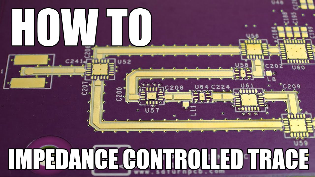
여기에서 이 주제에 대한 비디오를 시청하십시오. 주의 깊게 살펴보고 읽고 있는 내용에 대한 피드백을 제공하세요!
d여기에서 SDG #154 How to do controlled impedance traces on your PCB – pcb impedance head 주제에 대한 세부정보를 참조하세요
$5 for 2 layer PCBs with 24hr turnaround at https://www.pcbway.com/
Patreon: https://www.patreon.com/sdgelectronics
A big thank you to all of my Patreon supporters!
Soldering Tools and Equipment:
Solder Paste: https://bit.ly/2E1P5jR
Solder Flux: https://bit.ly/2MQn7we
Quick 857DW+ Hot Air Station: https://bit.ly/2OWDvf4
T12 Soldering Station: https://www.banggood.com/custlink/3KK3rVZu53
AC Version: https://www.banggood.com/custlink/3GK3C581V0
T12 Iron Tips: https://www.banggood.com/custlink/3DG3CHZ1SD
Daniu Tip Cleaner: https://bit.ly/31VHwWM
KSGER T12-BCM3 Tip: https://bit.ly/2xgYXCQ
Test Equipment:
Mustool MDS8207 Multimeter: https://bit.ly/2kKHr7A
FY6900 Generator: https://bit.ly/2yZI40n
Differential Probe: https://bit.ly/31xNTOF
Microscope Equipment:
Eakins Barlow Lenses: https://bit.ly/3aBY5tR
Eakins Black Microscope: https://bit.ly/2VEcYaW
Eakins Camera Microscope: https://bit.ly/2x86hnT
Camera Adaptor for Microscopes: https://bit.ly/2KBZQMQ
Amscope Microscope Head (US): https://amzn.to/2YmZWNx
Amscope Trinocular Microscope (US): https://amzn.to/2YdBE8k
Amscope Trinocular Microscope (UK): https://amzn.to/2V8w9Gh
Swift SS41-WF20 Binocular Microscope US: https://amzn.to/2VLWEpb
Swift SS41-WF20 Binocular Microscope UK: https://amzn.to/2GYGYFV
Visit my website: https://www.sdgelectronics.co.uk/
#cpwg #microstrip #50R #ElectronicsCreators
pcb impedance head 주제에 대한 자세한 내용은 여기를 참조하세요.
6. (a) Impedance Head PCB-288D01 (b) Shaker with …
Download scientific diagram | 6. (a) Impedance Head PCB-288D01 (b) Shaker with Impedance Head from publication: State Estimation of Lithium Ion Battery …
Source: www.researchgate.net
Date Published: 7/29/2022
View: 9699
Model 288D01 Mechanical Impedance … – PCB Piezotronics
PCB Industrial Monitoring and Measuring Equipment – China RoHS 2 Disclosure Table. 部件名称 … impedance head (also known as a driving point sensor) and.
Source: www.pcbpiezotronics.fr
Date Published: 9/8/2021
View: 2965
Model 288D01 Mechanical Impedance … – PCB Synotech GmbH
with any PCB product, PCB will repair, … the equipment to PCB Piezotronics for repair. … impedance head (also known as a driving point sensor) and.
Source: www.synotech.de
Date Published: 1/12/2022
View: 7495
Why So Important of PCB Impedance Control ? – RayMing
When the digital signal is transmitted on the board, the characteristic impedance of the PCBtrace must match the electronic impedance of the head and tail …
Source: www.raypcb.com
Date Published: 9/6/2022
View: 5734
PCB Impedance Calculator | Microstrip, Stripline…
With this PCB Impedance Calculator from Omni, you can calculate in … Omni has it all, except that fantastic ea that’s in your head.
Source: www.omnicalculator.com
Date Published: 3/21/2022
View: 7850
주제와 관련된 이미지 pcb impedance head
주제와 관련된 더 많은 사진을 참조하십시오 SDG #154 How to do controlled impedance traces on your PCB. 댓글에서 더 많은 관련 이미지를 보거나 필요한 경우 더 많은 관련 기사를 볼 수 있습니다.
주제에 대한 기사 평가 pcb impedance head
- Author: SDG Electronics
- Views: 조회수 20,441회
- Likes: 좋아요 677개
- Date Published: 2020. 5. 10.
- Video Url link: https://www.youtube.com/watch?v=861qZagBmqs
Why So Important of PCB Impedance Control ?
Rayming provide impedance control PCB manufacturing, We accept multi-impedance control design, exactly manufacturing control with strip sample and impedance test report, Send your PCB files to [email protected], Estimate Cost Now !
What is impedance control PCB?
Impedance Control PCB is the characteristic impedance of a transmission line formed by PCB conductors. It is relevant when high-frequency signals propagate on the PCB transmission lines. PCB Impedance Control is important for signal integrity: it is the propagation of signals without distortion.
PCB impedance control
Controlled impedance in the fabrication and design of PCB is a complex and broad topic. Therefore, understanding it could be somehow tricky.
If you are new to this, or you are searching for some information on the topic, then this guide will be of help to you. You’ll understand the hows, whys, and whats of impedance control. Please continue reading.
Controlled Impedance: What Does This Mean?
This is a good question. For us to understand what controlled impedance is, let us first of all define what impedance is. Impedance has to do with the degree at which the energy flow in a transmission line or electric circuit is opposed.
This is measured in Ohms and is represented as Z. This is the result when the reactance (X) and the resistance (R) are summed up. The reactance here is the result of two effects, which includes:
The capacitance, which is the storing of electrostatic charges as a result of the conductors’ voltages
The Inductance, which induces voltages in capacitors as a result of the currents’ magnetic fields
Usually, at DC, there is no reactance, and the copper’s resistance is typically trivial. For the high-speed AC circuits, the impedance and reactance becomes very important. Here, impedance can be critical due to the functionality of the design.
This is because impedance changes along the path of the signal from the transmitter to the receiver could lead to glitches, as well as a reduction in the performance of the system. Controlled impedance can be defined as a design technique, which assures that mismatches of the impedance in a circuit falls within limits that are tolerable.
Impedance control PCB is therefore a circuit board design having features which can control mismatches of impedance.
Characteristics of Impedance in PCBs
A PCB trace impedance comes with several features to look into concerning impedance. The features of a 50 ohm PCB trace PCB board design impedance include: dielectric constant, length, width, height, PCB fabrication limits/tolerances, and the distance between the track & other copper features.
These are the characteristics to look into when manufacturing impedance control PCBs and when calculating it.
Why Is Impedance Control PCB Necessary?
Recently, we’ve seen a continuous rise in device switching speeds. Generally, these devices have suddenly become complicated and faster. For instance, signal integrity issues have now become very repetitive with an increase in the operational speeds of devices. This means that the devices of today must be able to solve any SI issues.
Therefore, you cannot keep treating PCB traces as point-to-point connections. Rather, begin to consider them as transmission lines. Also, you must understand the importance and necessity of impedance matching in getting rid of or reducing the effect on SI. Know that, by working with good design approaches and practice, you can easily prevent possible SI issues. In this case, controlled impedance can assist you in mitigating or averting SI issues.
Other reasons why you need impedance control PCB includes
More Signal Power Required
PCB trace functions to transfer a driver device’s signal power to a device that will receive it. Here, power has to be transmitted all through the trace’s length. However, maximum signal power can only be achieved with the PCB’s matching impedances.
This is one reason why an impedance control PCB is needed. This type features an impedance matching, which permits enough power from the driver of the device and ends at the receiver.
Improved Performance
If you are searching for a PCB, which ensures quality device performance, then you should choose impedance control PCB.
One reason why the majority of devices fail when it comes to integrity and signal power is as a result of poor PCB layout and design. The layout stage during the manufacturing of PCB is usually a very critical one. If one is not careful, there’s a high chance that there will be a degradation of high-speed signals as they propagate to the receiver.
Devices that are controlled by impedance control PCB usually utilize less energy and perform faster. This PCB type allows devices to function better for long, thereby improving their control reliability and value.
Control flow of Energy
It’s true that impedance control PCB makes use of less energy. However, if you also need to control the flow of energy in your projects, then one great choice is impedance control PCB. The fact is, controlled impedance is important when transitioning from lower to higher ohm environments where there is impedance.
Why is this so? These transitions could result in reflection of energy to look like powerful and strong pulses. These pulses can disrupt the flow of energy. Therefore if your application deals with digital devices that work with high power, like those of RF applications, then it becomes necessary to use impedance control PCB.
Managing Electromagnetic Interference
If you use impedance control PCB, then you don’t have to worry about circuit disruptions, as a result of electromagnetic interference.
Concerning the PCB world, a pulse of reflection energy can disrupt circuits completely. This disruption usually extends to neighboring components. Also, there is a strong potential to interrupt the flow of energy and cause product operation failure.
Calculating Controlled Impedance in PCBs
To ensure signal integrity in PCB designs with high-speed, there’s a need for great impedance characteristics in the connections of the conductor trace.
These can only be determined after the PCB’s controlled impedance is calculated based on the impedance specifications, layout, and layer buildup.
What results is slight changes of the stackup and the relevant conductor geometries. Note that a PCB’s impedance is majorly influenced by:
Trace width
Permittivity
Copper thickness
Conductor geometries
The signal layer’s distance
Making use of simple equations, you can now calculate for controlled impedance. This will help in obtaining nominal values of impedance’ trace dimensions. These equations are very important for spacing and line widths higher than 15mil.
These simple equations are just approximations. Normally, they don’t give the best results utilized on PCBs of current technology. Besides, these equations usually need complex mathematics. Due to this reason, to determine PCB controlled impedances, utilize a PCB impedance calculator.
You can get some of these calculators online. Just choose one you can easily work with and make sure that you input the right calculation values. Remember that, whatever results are shown by these calculators are uniquely for rough estimation and approximation.
The manufacturer should calculate the corresponding layer construction, and impedance.
Specifying of PCB Impedance
Usually, manufacturers of PCB will deliver standard stack up. This will be utilized to calculate, either through software or by hand, what the trace dimension be with reference to this stack up.
If your results are plausible, then make use of them. Other than this, you’ll have to indicate the stack up that suits your needs. How can this be achieved?
Begin with a practical trace thickness for manufacturability, spacing, routing. Also compute the dielectric thickness, given that there is a material with the right with a specific dielectric constant, for your required impedance.
For the right options of prepreg sheets and core thickness, make sure you pick the closest type. Immediately you achieve this, recalculate your trace dimensions. If you are using software, and it permits it, check that the SI is okay and stimulate the critical lines.
Remember that this requires trace dimensions, driver model, and stackup specifications. It will also require whichever vias you may be using, as well as their dimensions. Also, correct these accordingly; you’ll have the trace and stackup dimensions for the needed impedance.
Now, the next thing for you to do is to deliver the information to your manufacturer. To achieve this, just draw a representation of a similar thickness. You can include some notes that specify your desired dielectric material and constant.
Designing Impedance Control PCB
The initial step in designing your PCB is the schematic capture. Just the same way you will draw on paper, draw a conceptual circuit. Then for each circuit’s symbol, give it a footprint. A footprint is the component’s physical package.
After the footprint is assigned, the CAD program used will generate a netlist. A netlist can be referred to as your schematic’s flat representation, which is usually machine-readable. It gives a unique ID to each footprint’s pin.
In addition, given your schematics, it creates a rundown of the connections between the nodes. At this point, you’ll be opportune to perform the layout of the actual design.
Generally, your circuit board needs to be very small. Also, you’ll want this option to suit all the connections needed at your desired widths. For this, you’ll require wider traces, because it is a high-speed circuit.
Making use of more layers means making the signal clearer is possible, as well as reducing the size of the PCB. After the layering is completed, you can then go ahead to place components beginning with those having physical constraints.
Let’s say your board has connects, LEDs, or switches, they have to be positioned to match the box’s cut out holes. You’ll then continue by placing the complicated and large ICs in a way that reduces the required traces.
At this point, you can place the different components supporting everything already explained above. Finally, you can go ahead to create traces (wires), which connect pads/pins, which should be connected. Here, CAD programs play an important role because they can check for error making use of netlist.
Conclusion
I hope you have been able to find answers to questions running through your mind regarding impedance control PCB. As mentioned earlier, to understand impedance as well as problems surrounding impedance control are not that easy.
Nonetheless, we have done our best to explain the topic deeply, and at this point, I believe you have become an expert on impedance control PCB.
The impedance of the circuit board is determined by the physical dimensions (line wide/space) and materials of the circuit and is measured in Ohms (Ω).
PCB impedance control has been one of the essential concerns and challenging problems in high-speed PCB design. As an impedance control designer, you should know what affect PCB impedance and how to calculate impedance.
1.The following parameters largely determine the impedance of a PCB:
1) Distance of signal layer and potential
2) Conductor geometry
3) Trackwidth
4) Copper thickness
5) Permittivity εr
2.Impedance and Delay Calculation Formula of Transmission Lines on PCB
Formula Restrictions:0.1 < w/h < 3.0 Formula Restrictions:0.1 < w/h < 3.0 Formula Restrictions:0.1 < w/h < 3.0 Formula Restrictions:0.1 < s/h < 3.0 Here is some free PCB software that provides impedance control calculations and online calculators as a reference. Selecting Foil-Built or Core-Built PCBs to Support Impedance Control RayMing Technology normally suggests impedance designers choose Foil-Built PCBs in order to make the most economical PCB. That being said, our Prototype PCB Assembly is very flexible, and we can use Core-Built PCBs. Foil-Built PCBs not only tend to be more economical than Core-Built PCBs, but they are also slightly easier to fabricate. The pictures below explain the differences between the Foil-Built and Core-Built PCBs. Foil-Built PCB board uses one less core than the Core-Built PCBS in the stack-up. The outside consists of aluminum foil. In addition, foil in different copper weights is much easier to purchase. Since Foil-Built PCBs are made of aluminum, they can be used on any builds, regardless of the primary laminate material used. PP (Pre-pregs) are also less costly than cores, especially if they are 5 mil or thinner. Core-Built PCB board has cores on the outside, so there is no need to use aluminum foil. Depending on material availability, it may be difficult to acquire a core with uneven copper weights. This forces the PCB manufacturer to etch down the cores, which is costly since a good deal of labor is involved. Except for labor, the PCB factory must use a higher copper weight than what appears on the board, increasing material cost. Nowadays, PCB designs and electronic components become smaller, faster – in other words, more complicated. PCB Impedance Control is becoming more critical. RayMing has ten years of PCB manufacturing experience, and we can provide full support when designing a PCB impedance board. PCB Impedance Design and calculator 1.Main types and affecting factors of PCB impedance design The opposition encountered during current transmission in a DC circuit is called resistance, and the opposition encountered by the current in an AC circuit is called impedance. The opposition encountered by the transmission signal in the high frequency (>400MHZ) circuit is called the characteristic impedance. In high frequency, the transmission signal copper wire on the PCB can be regarded as a conductive line composed of a series of equivalent resistance and a parallel inductance. This equivalent resistance is as small as it can be ignored. Therefore, when we analyze the signal transmission of a PCB at high frequency, we only need to consider the effects of the stray distribution of series inductance and parallel capacitance. We can get the following formula:
Z0=R+√L/C√≈√L/C (Z0 is the characteristic impedance value)
When the digital signal is transmitted on the board, the characteristic impedance of the PCBtrace must match the electronic impedance of the head and tail components. If it does not match, the transmitted signal energy will be reflected, attenuated, delayed, or lost, resulting in miscellaneous messages.
The higher the electronic impedance of the electronic component, the faster its transmission rate, so the characteristic impedance value of the circuit board must be increased accordingly to match it.
In addition to Z0, the PCB used for radio frequency communication sometimes emphasizes the board itself has a low Er (dielectric constant) value and a low Df (dielectric loss factor) value. The transmission speed of high-frequency signals in the medium is C/Er. It can be seen that the smaller the Er, the faster the transmission speed, which is why high-frequency materials with a low dielectric constant are used. Df affects the distortion of the signal in the medium transmission process. The smaller the Df, the smaller the distortion.
With the development of science and technology, especially the advancement of integrated circuit materials, the computing speed has significantly improved. It also promotes the integration of integrated circuits towards high density, small volume, and single parts. These are the reasons that lead to a high frequency of future PCB materials. The use of high-speed digital circuits means that the impedance of the circuit must be controlled, low distortion, low interference, low crosstalk, and elimination of electromagnetic interference (EMI). Impedance design is gradually crucial in PCB design. In PCBs with high-frequency signal transmission, the control of characteristic impedance is critical, and characteristic impedance is the core of solving signal integrity problems. At the front-end of PCB manufacturing, the front part of the system is responsible for the simulation calculation of impedance and the design of the impedance bar. Customers have become more stringent in impedance control. The number of impedance controls has increased how to quickly and accurately design impedance is a problem that greatly concerns PCB designers.
2.Main types and affecting factors of impedance
Impedance(Z0) definition: The total opposition to an alternating current flowing through it at a known frequency is called impedance(Z0). For PCBs, it refers to the total opposite of a certain circuit layer (signal layer) to its closest reference plane under high-frequency signals.
The types of impedance
Characteristic impedance
In electronic information products such as computers and wireless communications, the energy transmitted in the PCB circuit is a square wave signal composed of voltage and time. The opposition it encounters is called characteristic impedance.
Differential Impedance
Two identical signal waveforms with opposite polarities are input at the driving end, respectively transmitted by two differential lines, and the two differential signals are subtracted at the receiving end. Differential impedance is the impedance between two lines.
Odd-Mode Impedance
The impedance of one line to the ground is the same as the second line.
Even-mode impedance
Impedance when two same signal waveforms with the same polarity are input at the drive end, and the two wires are connected.
Common-mode impedance
The impedance of one of the two lines to the ground is the same as the impedance of the two lines; it is usually greater than the odd mode impedance.
Among them, characteristic impedance and differential impedance are common impedance, and common-mode impedance and odd-mode impedance are rare.
Analysis of the factors affecting impedance from the perspective of PCB manufacturing
W — Line width/line space: The line width increases, the impedance decreases, and the distance increases, the impedance increases.
H — Insulation thickness: the thickness increases, and the impedance increases.
T — Copper thickness: the copper thickness increases, and the impedance decreases.
H1 — Solder mask thickness: the thickness increases, and the impedance decreases.
Er — The dielectric constant: the DK value increases, and the impedance decreases.
Undercut — W1-W: the undercut increases, and the impedance increases.
In addition, when the surface process is immersion-gold (or gold plating), the etching process of the outer layer is different from other surface processes, and the line compensation is different. The impedance calculation result of the former will be 3-5 ohms larger, so the resistance value of the gold plating process and other process switching needs to be adjusted.
3.Impedance calculation automation
The most commonly used impedance calculation tool in our industry is the Si8000 Field Solver provided by Polar. Si8000 is a brand-new boundary element method field-effect calculator software. It is based on the easy-to-use user interface of the early Polar impedance design system we are familiar with. This software contains various impedance modules, and personnel can calculate impedance results by selecting specific modules, inputting related data such as line width, line spacing, inter-layer thickness, copper thickness, and Er value. A PCB impedance control number can be as few as 4 to 5 groups or as many as dozens of groups. The control line width, inter-layer thickness, copper thickness, etc., of each group are also different. If you check the data one by one and then manually input the relevant parameters and then calculate, it is time-consuming and error-prone.
To ensure the quality of signal transmission, reduce EMI interference, and pass relevant impedance testing and certification, it is necessary to conduct an impedance matching design for PCB key signals. Considering common calculation parameters, TV product signal characteristics, PCB Layout actual needs, SI8000 software calculations, PCB supplier feedback information, etc., finally come to this recommended design. It is suitable for most PCB suppliers’ process standards and PCB board design with impedance control requirements.
1).Two Layer Impedance Design
100 ohm differential impedance recommended design
Ground package design: line width/spacing 7/5/7mil ground wire width ≥20mil signal and ground wire distance 6mil, add ground vias every 400mil.
Design without ground package: line width/spacing 10/5/10mil, the distance between the differential pair and the pairis ≥20mil (not less than 10mil in special cases). It is recommended that the entire group of differential signal lines is shielded with grounding, and the distance between the differential signal and the shielding ground ≥35mil (not less than 20mil in special cases).
90 ohm differential impedance recommended design
Ground package design: line width, line spacing 10/5/10mil ground wire width ≥20mil signal and ground wire distance 6mil or 5mil, add ground vias every 400mil
Design without ground package: line width, line spacing 16/5/16mil, the distance between the differential pair and the pairis ≥20mil, it is recommended that the entire group of differential signal lines should be shielded with ground, and the distance between the differential signal and the shielding ground ≥35mil (In special cases, it cannot be less than 20mil).
Note: Prioritize the use of package ground design. However, if the line is short and there is a complete ground plane, it can be designed without package ground.
Calculation parameters:
FR-4, thickness 1.6mm+/-10%, dielectric constant 4.4+/-0.2, copper thickness 1.0 oz (1.4mil), solder mask thickness 0.6±0.2mil, dielectric constant 3.5+/-0.3.
Fig.1 Design of ground package Fig.2 Design without ground package
2) Four Layer impedance design
100 ohm differential impedance recommended design
line width, spacing 5/7/5mil differential pair and the distance between the pair ≥ 14mil (3W criterion);
Note: It is recommended that the entire group of differential signal lines is shielded with ground, and the distance between the differential signal and the shielded ground line is ≥35mil (in special cases, it cannot be less than 20mil).
90 ohm differential impedance recommended design
line width, spacing 6/6/6mil differential pair, and the distance between the pair ≥12mil (3W criterion).
Note: In the case of a long differential pair trace, it is recommended that the USB differential line wrap the ground at a distance of 6 mils on both sides to reduce the risk of EMI (with and without ground, the line width and line spacing standards are consistent).
Calculation parameters:
FR-4, thickness 1.6mm+/-10%, dielectric constant 4.4+/-0.2, copper thickness 1.0 oz (1.4mil), copper clad substrate(PP) 2116 (4.0-5.0mil), dielectric constant 4.3+/-0.2, solder mask thickness 0.6±0.2mil, dielectric constant 3.5+/-0.3.
Stack-up:
Silkscreen Solder mask Copper Prepreg Base material Prepreg Copper Solder mask Silkscreen
3) Six Layer impedance design
The impedance design of the outer trace is the same as that of the four layer board.
The inner trace is generally more plane layer than the surface trace, and the electromagnetic environment is different from the surface.
The following is the third layer trace impedance control recommendation.
100 ohm differential impedance recommended design
line width, spacing 6/10/6mil.
The distance between the differential pair is ≥20mil (3W criterion).
90 ohm differential impedance recommended design
line width,line spacing 8/10/8mil.
The distance between the differential pair is ≥20mil (3W criterion).
Calculation parameters:
FR-4, thickness 1.6mm+/-10%, dielectric constant 4.4+/-0.2, copper thickness 1.0 oz (1.4mil), copper clad substrate(PP) 2116 (4.0-5.0mil), dielectric constant 4.3+/-0.2, solder mask thickness 0.6±0.2mil, dielectric constant 3.5+/-0.3.
Stack-up:
Silkscreen Solder mask Copper Prepreg Base material Prepreg Base material Prepreg Copper Solder mask Silkscreen
For layersmore than six layers, please design by yourself according to relevant rules or consult relevant personnel to determine the stack-up and trace If there are other impedance control requirementswith special circumstances, please calculate by yourself or consult relevant personnel for alternative design solutions.
Note:
Many situationsaffect impedance, and PCBs that require impedance control still need to indicate impedance control requirements in the PCB design data.
100 ohm differential impedance is mainly used for HDMI and LVDS signals, among which HDMI mustpass relevant certification.
90 ohm differential impedance is mainly used for USB signals.
Single-ended 50 ohm impedance is mainly used for some DDR signals. Giventhe large DDR particles, some adopt an internally adjusted matching impedance design. The design is based on the demo board provided by the solution company. This design guide is not recommended;
Single-ended 75 ohm impedance is mainly used for analog video input and output. There is a 75 ohm resistor in the circuit design to match the ground resistance, so there is no need to perform an impedance matching design in the PCB Layout. Still,you need to pay attention to the 75 ohm grounding resistance in the circuit that should be placed close to the terminal pin.
PP types
Type Dielectric thickness Adjustable range Dielectric constant 1080 2.8mil 2.0-3.0mil 4.3 2116 4.2mil 4.0-5.0mil 4.3 1506 6.0mil 5.5-6.5mil 4.3 7628 7.2mil 7-8.5mil 4.3
Solder mask thickness: 0.6±0.2mil
Cer=3.5+/-0.3
Impedance Test:
Impedance test receives the reflected wave simultaneously after the oscilloscope sends out a pulse wave, then compares and analyzes the two pulse waves, and gets the impedance value from the reflected energy.
Impedance test schematic
Using TDR (Time Domain Reflectometry) measurement, the general measurement method uses “time domain reflectometry.”
The calculation formulas of some impedance types are introduced above, but the current impedance is calculated by the software, which is faster and more accurate. Our factory currently uses Polar’s test instrument CITS500s.
Test range: 0-300ohm
Test accuracy: 1%—50ohm
1.25% — 75ohm
1.5% — 28\100ohm
Reflected Pulse Rise time: ≤200ps
System bandwidth: 1.75GHz
The dielectric constant Er will change with the working frequency. Within a specific range, the higher the frequency, the smaller the Er. Annex I, Annex II, and Annex III are core board Er provided by three sheet suppliers, which can be viewed at 1MHz. The dielectric constant is greater than that at 1GHz.
Characteristic impedance
It is composed of resistance and reactance (combined by inductive reactance and capacitive reactance). The characteristic impedance in the PCB depends on the width and thickness of the wire, the distance between the wire and the ground plane, and the dielectric constant (εr) of the medium between the wires.
Impedancematch
The signal transmission in the electronic circuit starts from the output of the power supply. It expects to be transmitted to the receiving end without energy loss and any signal reflection in the middle.
Therefore, the impedance (ZL) in the PCB is required to be equal to the impedance (ZO) of the power supply terminal, which is called impedance matching. If the impedance cannot be matched, the received signal is distorted.
A transmission line structure in which the wires are parallel to the ground plane in the PCB and separated by the medium.
Strip-line
A strip-line is a high-frequency transmission wire between two parallel ground planes (or power planes) between dielectrics.
PCB Impedance coupon design
In the circuit, the ratio of voltage to current in the transmission wave between two points, including the assembled components, is the resistance of any point of the transmission line to the transmission wave.
Square PAD “■”——The outer layer of PTH corresponds to PAD, and the inner and outer layers of this PTH are only connected to the relevant shielding layer.
RoundPAD “●”——The outer layer of PTH corresponds to PAD, and the inner and outer layers of this PTH are only connected to the signal lines of the relevant layer.
A font is added next to each outer round pad and square pad to indicate the layer sequence of the signal line layer or shielding layers. For example,1, 2, 3, 4, 10, and 11 represent the signal layer or shielding layer in the first, second, third, tenth, and eleventh layer.
Except for the gong pipe position hole, the other holes are made of PTH, and the upper pad or round pad is added accordingly.
When there is more than one impedance baron Wpnl, add different numbers 1, 2, 3, 4, etc., to the circuit layer/silkscreen layer for identification during testing and analysis.
The PTH hole diameter of each impedance baris uniformly φ1.00mm, and two gong pipe holes φ1.60mm should be added.
When there is a need for production layout or additional control of impedance lines is required, a single-hole connection signal line design can be used. See P4 and P5 diagrams to save design positions.
Suppose the impedance bar is designed in a range with a small length (sometimes,the customer will specify the location). In that case, the signal line can be in a turning form to ensure the total signal line. It is important to avoid right-angles in wiring and maintain a large turning radius. The length is sufficient (refer to the tenth requirement at the same time). Still, the signal line distance should be kept above 2.54mm. See figure P8.
If there are no special requirements, the gap between the signal line and the DummyPattern is five times the minimum distance (mm) to the shielding layer.
For non-coplanar type impedance bars, if the customer does not specify requirements when designing the impedance bar, the Dummy Pattern next to the signal line (the distance between the long copper bar or copper pad and the signal line, t, must be ≥5H (H is the signal layer to the shield) The insulation thickness or minimum thickness of the layer). The following examples illustrate.
Note: For non-coplanar type impedance, when the distance between the Dummy Pattern and the copper skin is less than 5t, the impedance will become smaller as the distance becomes smaller, even if other conditions have not changed.
A.For Microstrip type, t = insulation thickness from the signal layer to the shielding layer.
B.The Stripline type, t=the smaller of the insulation thickness from the signal layer to the two shielding layers H1 and (H-H1-T). t = the insulation thickness min.
*Differential impedance is handled in the same way
Note: Not only the distance between the signal line and the Dummy Pattern in the same layer must be made according to the above requirements, but also in the situation in the following figure. When L3 has impedance control requirements, the signal line of the L3 layer is in the other layer (the figure is L4 as an example). The spacing t of Dummy Pattern should also be made according to the above requirements.
As for the impedance of the coplanar type, the designer (customer) specifies the spacing. The spacing between the signal line and the copper coupon next to it – is a component of the coplanar type impedance, which cannot be agreed upon by the customer and cannot be changed. To ensure proper spacing, the next copper wires or large copper bars should also be vibrated thick.
Single-line or double-line impedance, each with 2 or 4 test holes, must ensure that the relative distance between their hole centers remains unchanged(see P); otherwise, the test cannot be performed. It is 2.50mm), the hole size is 0.8mm to 30 mm (refers to the customer to design. Please refer to the fifth requirement for factory design). If the customer has designed a test pattern in the PCB, the relevant PPE personnel will check whether the design is suitable for the test instrument requirements of the factory. If it is not suitable, consult the customer to change the design to facilitate the factory test. If there are disagreements, one can also design a coupon to be able to test.
In general, the length of the signal cable should be 6″ or more.
If there areno special instructions, for all large copper skins, the inner layer is 0.50mm from the outer shape of the Coupon, and the outer layer is 0.30mm from the outer shape of the Coupon.
For the pads added by the innerand outer layer to the PTH, ensure that AR=0.25mm. For the inner layer, cut out copper for non-connected holes, ensure that Clearance=0.30mm (all layers are also made of copper for gong pipe positions). Solder the solder mask Pan and gong pipe position hole plus window, one side larger 0.10mm.
Vibration according to MI and film production instructions.
Unless the customer requires, do not design the impedance bar in the Unit/Set.
Place the impedance baras close as possible to the control line in the PCB. This is to make the control line on the impedance bar after plating and etching have better consistency with the copper thickness and line width in the PCB. Arrange this position in the middle area of the layout.
See P — P for standard graphics. According to different line width, impedance,and pressure plate requirements, select the corresponding graphic combination and make the corresponding connections and adjustments, and the design will be completed.
The current analysis of the impedance bar is to slice at three positions at both ends and the middle and detect the following: copper thickness, the upper and lower top widths of the circuit, and the average value of the insulating layer thickness (some need to add the thickness of the solder mask). Then add the measured impedance value and compare it with the designed theoretical value to determine whether the impedance is okay.
Impedance control difficulties
Medium thickness
Uneven pattern distribution results in an uneven thickness of the medium, fluctuations in impedance, and discontinuity.
Line width
The line width/line spacing is getting smaller and smaller, and the line width accuracy is getting more challenging to reach ±10%.
Outer layer electroplating unevenness – The copper thickness is affected by electroplating parameters, uneven pattern distribution, hanging board method, and other factors. The thickness of different patterns varies greatly, resulting in inconsistent line width.
The future development trend of impedance control
PCB Impedance Calculator
I know, I know, that was a bit cheesy, I admit it. But it is also true. With this PCB Impedance Calculator from Omni, you can calculate in seconds your microstrip impedance or the impedance of a variety of conductors in a PCB. Of course, you can also do it by hand if you really wanted to; the literature referenced at the end of this article has all the equations we used.
But if you’re trying to get your project done and your PCB designed, there is no need to waste time and effort in those tedious calculations. Using this Omni calculator is extremely simple. All you need to do is choose the type of conductor you are dealing with, fill in the geometric measurements of your setup, and it will automagically give you the relevant impedance (or impedances) based on your input.
We have a wide variety of conductors for you to choose from. The complete list is here:
Microstrip
Edge-coupled microstrip
Wire microstrip
Embedded microstrip
Edge-coupled stripline
Broadside-coupled stripline
Symmetric stripline
Asymmetric stripline
If you’re unsure of which one you have, don’t worry because the calculator will show you a diagram of your selected type of conductor explaining every geometric parameter you need to calculate the impedance.
Emerging Challenges for Experimental Mechanics in Energy and Environmental …
0 Bài đánh giá Google không xác minh bài đánh giá nhưng có kiểm tra để tìm nội dung giả và xoá nội dung đó khi tìm thấy Viết bài đánh giá
Emerging Challenges for Experimental Mechanics in Energy and Environmental … được biên tập bởi Amalia Martínez-García, Cosme Furlong, Bernardino Barrientos, Ryszard J. Pryputniewicz
키워드에 대한 정보 pcb impedance head
다음은 Bing에서 pcb impedance head 주제에 대한 검색 결과입니다. 필요한 경우 더 읽을 수 있습니다.
이 기사는 인터넷의 다양한 출처에서 편집되었습니다. 이 기사가 유용했기를 바랍니다. 이 기사가 유용하다고 생각되면 공유하십시오. 매우 감사합니다!
사람들이 주제에 대해 자주 검색하는 키워드 SDG #154 How to do controlled impedance traces on your PCB
- pcb
- 50R
- impedance
- cpwg
- coplanar
- microstrip
SDG ##154 #How #to #do #controlled #impedance #traces #on #your #PCB
YouTube에서 pcb impedance head 주제의 다른 동영상 보기
주제에 대한 기사를 시청해 주셔서 감사합니다 SDG #154 How to do controlled impedance traces on your PCB | pcb impedance head, 이 기사가 유용하다고 생각되면 공유하십시오, 매우 감사합니다.