
You are looking for information, articles, knowledge about the topic nail salons open on sunday near me end cap cells in vlsi on Google, you do not find the information you need! Here are the best content compiled and compiled by the https://chewathai27.com/to team, along with other related topics such as: end cap cells in vlsi Don t touch cells in vlsi, Tie cells in VLSI, Clamp cells in VLSI, Tap cell in VLSI, Endcap in vlsi, Always on cells in VLSI, End cap in VLSI, Physical cell in vlsi
The end cap cell or boundary cell is placed at both the ends of each placement row to terminate the row. It has also been placed at the top and bottom row at the block level to make integration with other blocks. Some standard cell library has also corner end cap cells to place the corner of the block.Boundary cells protect your design from external signals. These cells ensure that gaps do not occur between the well and implant layer and to prevent from the DRC violations.The tie cell is a standard cell, designed specially to provide the high or low signal to the input (gate terminal) of any logic gate. The high/low signal can not be applied directly to the gate of any transistors because of some limitations of transistors, especially in the lower node.
Table of Contents
Why boundary cells are used in VLSI?
Boundary cells protect your design from external signals. These cells ensure that gaps do not occur between the well and implant layer and to prevent from the DRC violations.
What is tie cells in VLSI?
The tie cell is a standard cell, designed specially to provide the high or low signal to the input (gate terminal) of any logic gate. The high/low signal can not be applied directly to the gate of any transistors because of some limitations of transistors, especially in the lower node.
What is clamp cell in VLSI?
We also refer to isolation cells in VLSI as clamp cells. An isolation cell is necessary in low power architecture when each logic signal passes from a power domain that can be turned down to a domain that cannot be powered down.
What is the purpose of endcap?
Those displays that are set up on the ends of aisles, sometimes every aisle, are end caps. They cap the end of each aisle in an attractive, eye-catching way to help buyers notice commonly purchased products that they may need on their visit.
What is end cap cells?
The end cap cell or boundary cell is placed at both the ends of each placement row to terminate the row. It has also been placed at the top and bottom row at the block level to make integration with other blocks. Some standard cell library has also corner end cap cells to place the corner of the block.
What are leaf cells in VLSI?
In a hierarchical design of a complex chip the leaf cells are the functional units at the lowest level of the hierarchy. A leaf cell (which is also called cell or circuit) realizes simple logical functionality and is built from a small number of transistors, usually not more than 30.
What is tap cell?
Well tap cells (or Tap cells) are used to prevent the latch-up issue in the CMOS design. Well tap cells connect the nwell to VDD and p-substrate to VSS in order to prevent the latch-up issue.
What are spare cells and why it is used?
Spare cells are basically elements embedded in the design which are not driving anything. The idea is that maybe they will enable an easy (metal) fix without the need of a full redesign.
What is tie high?
It refers to the number of boxes/cartons stored on a layer, or tier, (the TI) and the number of layers high that these will be stacked on the pallet (the HI). It can also be used in reference to the stacking pattern used to load a pallet in order to generate a relatively stable stack.
What are ESD cells?
ESD cells are protection circuits which protect the device from Electro static discharge.
What are preplaced cells?
The critical cells are mostly the cells related to clocks, viz. clock buffers, clock mux, etc. and also few other cells such as RAM’s, ROM,s etc. Since, these cells are placed in to core before placement and routing stage, they are called ‘preplaced cells’.
What is Crosstalk in VLSI?
Crosstalk is a phenomenon, by which a logic transmitted in vlsi circuit or a net/wire creates undesired effect on the neighbouring circuit or nets/wires, due to capacitive coupling.
What are end caps made of?
They are made from an LDPE with a neoprene or commercial rubber disc which is secure within the cap to make a good seal.
How wide is an end cap?
End-cap Booths are generally 10ft (3.05m) deep by 20ft (6.10m) wide. The maximum back wall height allowed is 8ft (2.44m) and the maximum backwall width allowed is 10ft (3.05m) at the center of the backwall with a maximum 5ft (1.52m) height on the two side aisles.
How effective are end caps?
There have only been a few studies that specifically examined the effectiveness of endcap sales uplift (Chevalier, 1975, Nakamura et al., 2014, Wilkinson et al., 1982). These studies established that endcaps are able to increase sales levels from 23% to an impressive 1197%.
What is a cell boundary?
The plasma membrane of the cell defines the cell boundary. It is the role of the plasma membrane to maintain the difference between the inside and the outside of the cell by controlling the entrance and exit of materials across the plasma membrane.
Where are border cells?
Boundary cells (also known as border cells or boundary vector cells) are neurons found in the hippocampal formation that respond to the presence of an environmental boundary at a particular distance and direction from an animal.
Where are boundary cells found?
Boundary cells, which are found in brain areas that provide input to the hippocampus, increase their firing at a preferred distance from a specific boundary.
What are spare cells and why it is used?
Spare cells are basically elements embedded in the design which are not driving anything. The idea is that maybe they will enable an easy (metal) fix without the need of a full redesign.
End Cap Cells in VLSI | Boundary Cells in VLSI – Team VLSI
- Article author: teamvlsi.com
- Reviews from users: 33634
 Ratings
 - Top rated: 3.4
- Lowest rated: 1
- Summary of article content: Articles about End Cap Cells in VLSI | Boundary Cells in VLSI – Team VLSI Updating …
- Most searched keywords: Whether you are looking for End Cap Cells in VLSI | Boundary Cells in VLSI – Team VLSI Updating
- Table of Contents:
Archives
Categories
PHYSICAL ONLY CELLS – VLSI- Physical Design For Freshers
- Article author: www.physicaldesign4u.com
- Reviews from users: 43567 Ratings
- Top rated: 3.8
- Lowest rated: 1
- Summary of article content: Articles about
PHYSICAL ONLY CELLS – VLSI- Physical Design For Freshers
Updating … - Most searched keywords: Whether you are looking for
PHYSICAL ONLY CELLS – VLSI- Physical Design For Freshers
Updating YOUR KEYWORDS HERE - Table of Contents:
Saturday December 28 2019
Pages
Pages
Translate
Followers
Labels
SOURCES
Popular Posts
Tie Cells in Physical Design – Team VLSI
- Article author: teamvlsi.com
- Reviews from users: 33830 Ratings
- Top rated: 3.4
- Lowest rated: 1
- Summary of article content: Articles about Tie Cells in Physical Design – Team VLSI Updating …
- Most searched keywords: Whether you are looking for Tie Cells in Physical Design – Team VLSI Updating
- Table of Contents:
Archives
Categories
What are Isolation Cells in VLSI? – ChipEdge VLSI Training Company
- Article author: chipedge.com
- Reviews from users: 8995 Ratings
- Top rated: 4.0
- Lowest rated: 1
- Summary of article content: Articles about What are Isolation Cells in VLSI? – ChipEdge VLSI Training Company Updating …
- Most searched keywords: Whether you are looking for What are Isolation Cells in VLSI? – ChipEdge VLSI Training Company Updating Isolation cells in VLSI are extra cells introduced by synthesis tools to isolate buses/wires crossing from a circuit’s power-gated domain to its always-on domain.
- Table of Contents:
Why Do We Require It
Isolation Cell Logic Design
Where Are Isolation Cells Placed
Conclusion
Sources
Image Source
Leave a Reply Cancel reply
Related Blog
Enquire Now
Enquire Now

PHYSICAL ONLY CELLS – VLSI- Physical Design For Freshers
- Article author: www.physicaldesign4u.com
- Reviews from users: 31186 Ratings
- Top rated: 3.5
- Lowest rated: 1
- Summary of article content: Articles about
PHYSICAL ONLY CELLS – VLSI- Physical Design For Freshers
Boundary cells consist of end-cap cells, which are added to the ends of the cell rows and around the boundaries of objects such as the core … … - Most searched keywords: Whether you are looking for
PHYSICAL ONLY CELLS – VLSI- Physical Design For Freshers
Boundary cells consist of end-cap cells, which are added to the ends of the cell rows and around the boundaries of objects such as the core … YOUR KEYWORDS HERE - Table of Contents:
Saturday December 28 2019
Pages
Pages
Translate
Followers
Labels
SOURCES
Popular Posts
Boundary Cap Cells/End Cap Placement – iVLSI
- Article author: ivlsi.com
- Reviews from users: 15281 Ratings
- Top rated: 4.8
- Lowest rated: 1
- Summary of article content: Articles about Boundary Cap Cells/End Cap Placement – iVLSI Boundary cap cells are physical only cells. These cells are placed at the periphery of the core and power domain. Boundary cap cells are placed … …
- Most searched keywords: Whether you are looking for Boundary Cap Cells/End Cap Placement – iVLSI Boundary cap cells are physical only cells. These cells are placed at the periphery of the core and power domain. Boundary cap cells are placed …
- Table of Contents:
Categories
Recent Posts
Leave a ReplyCancel Reply
VLSI DESIGN: END CAP CELLS
- Article author: vlsiwikipedia.blogspot.com
- Reviews from users: 20960 Ratings
- Top rated: 4.1
- Lowest rated: 1
- Summary of article content: Articles about VLSI DESIGN: END CAP CELLS End cap cells are placed on both ends of the horizontal site rows and also placed on top & bottom edges (nwell, DRC requirements). When these cells are placed … …
- Most searched keywords: Whether you are looking for VLSI DESIGN: END CAP CELLS End cap cells are placed on both ends of the horizontal site rows and also placed on top & bottom edges (nwell, DRC requirements). When these cells are placed …
- Table of Contents:
TOPICS
Total Pageviews
Contact
What is end-cap cell? What is about ensuring gaps not occuring between well or implant layers that could cause design rule violations? – Quora
- Article author: www.quora.com
- Reviews from users: 29841 Ratings
- Top rated: 4.8
- Lowest rated: 1
- Summary of article content: Articles about What is end-cap cell? What is about ensuring gaps not occuring between well or implant layers that could cause design rule violations? – Quora End-cap cell are physical only cells which are added to entify end of rows in digital chips or blocks.They are also added to isolate any analog IPs and … …
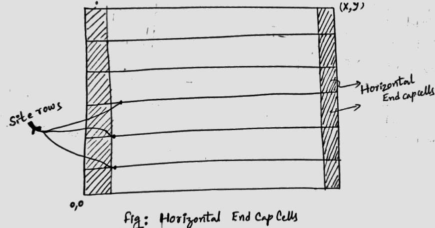
- Most searched keywords: Whether you are looking for What is end-cap cell? What is about ensuring gaps not occuring between well or implant layers that could cause design rule violations? – Quora End-cap cell are physical only cells which are added to entify end of rows in digital chips or blocks.They are also added to isolate any analog IPs and … ==> In short, these are used to address boundary Nwell issues for DRC cleanup These end cap cells will be placed on both ends of the horizontal rows and vertical rows. Usually there will be different cell for horizontal and vertical end cap purpos…
- Table of Contents:

Cells in PD | PD Essentials | Physical Design | VLSI Back-End Adventure
- Article author: vlsi-backend-adventure.com
- Reviews from users: 19985 Ratings
- Top rated: 3.2
- Lowest rated: 1
- Summary of article content: Articles about Cells in PD | PD Essentials | Physical Design | VLSI Back-End Adventure End Caps · End-cap cells are preplaced physical-only cells required to meet certaindesign rules and placed at the ends of the site rows by … …
- Most searched keywords: Whether you are looking for Cells in PD | PD Essentials | Physical Design | VLSI Back-End Adventure End Caps · End-cap cells are preplaced physical-only cells required to meet certaindesign rules and placed at the ends of the site rows by … Special Cell Requirements in IC Design is to minimize the possible CMOS issues, More no. of transistors than are necessary for basic functioning. e.g., â To limit the Overshoots and Undershoots
- Table of Contents:
Cells in Physical Design
Cells in Physical Design
Cells in ASIC Physical Design
VLSI Physical Design: End Cap Cells
- Article author: www.vlsijunction.com
- Reviews from users: 23052 Ratings
- Top rated: 3.8
- Lowest rated: 1
- Summary of article content: Articles about VLSI Physical Design: End Cap Cells End Cap Cells … These library cells do not have signal connectivity. They connect only to the power and ground rails once power rails are … …
- Most searched keywords: Whether you are looking for VLSI Physical Design: End Cap Cells End Cap Cells … These library cells do not have signal connectivity. They connect only to the power and ground rails once power rails are …
- Table of Contents:
Home
Tuesday 20 October 2015
Follow VLSI Junction on Social Media
Search This Blog
Contact Form
Translate
Blog Archive
Followers
end cap cells in physical design – howtogetclearskininamonth
- Article author: howtogetclearskininamonth.blogspot.com
- Reviews from users: 46722 Ratings
- Top rated: 4.4
- Lowest rated: 1
- Summary of article content: Articles about end cap cells in physical design – howtogetclearskininamonth They connect only to the power and ground rails once power rails are created in the design. End-cap cell are physical only cells which are added … …
- Most searched keywords: Whether you are looking for end cap cells in physical design – howtogetclearskininamonth They connect only to the power and ground rails once power rails are created in the design. End-cap cell are physical only cells which are added … end cap cells in physical design
- Table of Contents:
Iklan Atas Artikel
Iklan Tengah Artikel 1
Iklan Tengah Artikel 2
Iklan Bawah Artikel
Search This Blog
Label
Blog Archive
Postingan Populer
See more articles in the same category here: https://chewathai27.com/to/blog.
Boundary Cells in VLSI – Team VLSI
There are high chances to get damaged the gate of standard cells placed at the boundary during the manufacturing of chip. To prevent such damages at the boundary we have a special kind of cell in the standard cell library is called end cap cell or boundary cell. Boundary cell not only protects the gate damage at the boundary, but it also serves many other purposes. In this article, we will discuss the need for boundary cell placement, the structure and placement of boundary cells.
Where to place End Cap / Boundary Cells:
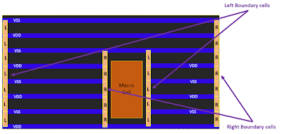
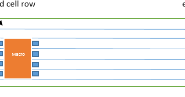
The end cap cell or boundary cell is placed at both the ends of each placement row to terminate the row. It has also been placed at the top and bottom row at the block level to make integration with other blocks. Some standard cell library has also corner end cap cells to place the corner of the block. Boundary cells have fixed attribute, therefore these cells can not be moved during the optimization. A typical placement of end cap cells at the end of the row has shown in figure-1.
Figure-1: Placement of end cap cell at the end of rows
Why need to place End Cap / Boundary Cell?
The end cap cells are placed in the design because of the following reasons:
To protect the gate of a standard cell placed near the boundary from damage during manufacturing.
To avoid the base layer DRC (Nwell and Implant layer) at the boundary.
To make the proper alignment with the other block.
Some standard cell library has end cap cell which serve as decap cell also.
Layout of end cap / boundary cell:
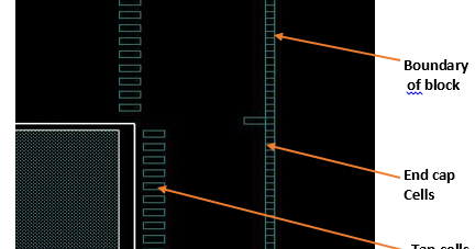
The boundary cell is a physical-only cell, has no logical functions and therefore these cells are not a part of the netlist. Boundary cells have mainly Nwell layer, implant layers, and dummy poly layer and metal rails as shown in the figure-2.
How to place:
VLSI- Physical Design For Freshers
Filler cell insertion is often used to add decoupling capacitors to improve the stability of the power supply and discontinuity in power.
Filler cells have no logical connectivity. these cells are provided continuity in the rows for VDD and VSS nets and it also contains substrate nwell connection to improve substrate biasing.
To ensure that all power nets are connected, you can fill empty space in the standard-cell rows with filler cells.
why we need continuity for nwell and implantation :
If there is continuity b/w nwell and implant layer it is easier for foundry people to generate them and the creation of a mask is a very costly process so it is better to use only a single mask.
If nwell is discontinuous the DRC rule will tell that place cells further apart i.e maintain the minimum spacing because there is a well proximity effect.
we know nwell is tap to VDD and P substrate is tap to VSS to prevent latchup problem. now if there is a discontinuity in nwell it will not find well tap cells, so we have placed well tap cells explicitly, therefore it will increase the area explicitly, hence we have filler cells so no need to place well tap cells.
when we placed filler cells in the design:
when optimization of clock tree synthesis is completed i.e after timing has been met because let’s say if we want to place buffer/inv for optimization purpose we can’t place these cells because there is already placed filler cells, and enough area is not there to present buffer/inv, so after timing has been met and routing optimization is done then only placed the filler cells to fill the empty space.
Well proximity effect:
During the manufacturing of chips, we will get these types of problems, that’s why they are second-order effects. In this, the transistors that are close to the well edge have different performance than ideally placed transistors, because of this effect the transistor speed can vary by +- 10%.
The transistor placed to the well boundary so it will get many problems during ion implantation. Implanted ion is coming to the well boundary and reflected/scatter from the well boundary to transistors Q1 & Q5 boundary and ions are deposited on the Q1 Q5 boundary. Ion particles are scattered/reflected due to photoresist on both side of nwell wall. these ions are deposited only those transistors who are near to the well boundary, so any one of the terminals of transistors gets affected by ion implantation and the rest of the transistor will get uniform ions.
well proximity effect
Tie Cells in Physical Design
The tie cell is a standard cell, designed specially to provide the high or low signal to the input (gate terminal) of any logic gate. The high/low signal can not be applied directly to the gate of any transistors because of some limitations of transistors, especially in the lower node. The limitation will also be discussed along with the schematic and operation of tie cells in this article. We will discuss the following sub-topics in this article.
Need of tie cells
Schematic of tie cells
The function of tie cells
Placement of tie cells
Need of tie cells:
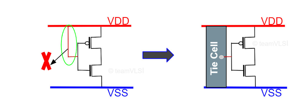
In the lower technology node, the gate oxide under the poly gate is a very thin and the most sensitive part of the transistor. We need to take special care of this thin gate oxide while fabrication (associated issue is antenna effect) as well as in operation too. It has been observed that if the polysilicon gate connects directly to VDD or VSS for a constant high/low input signal, and in case any surge/glitch arises in the supply voltage it results in damage of sensitive gate oxide. To avoid the damages mentioned above, we avoid the direct connection from VDD or VSS to the input of any logic gates. A tie cell is used to connect the input of any logic to the VDD or VSS.
Figure-1: Need of tie cell
There are two types of tie cells.
Tie-high cell
Tie- low cell
As the name suggests, the tie-high cell’s output is always high and the tie-low cell’s output is always low.
Schematic of tie cells:
The tie cell has no input pin and only one output pin. The output of the tie-high cell is always high and the output of the tie-low cell is always low and it is the glitch-free output that connects to the input of any logic gates. The schematic of tie high cell and tie-low cell is shown in the figure-2.
Figure-2: Tie-high and tie-low cells
In the tie-high cell, the drain and gate of nMOS are shorted together and connected to the gate of pMOS, and output is taken from the drain of pMOS. Whereas in the tie-low cell the drain and gate of pMOS are shorted together and connected to the gate of nMOS and output is taken from the drain of nMOS. The function of these schematics is explained in the next section.
Function of tie cells:
Both tie-high and tie-low cells have similar working. Here working of the tie-high cell is explained. A similar logic can think for tie-low cell. From figure-2 tie-high cell, the drain and gate of nMOS are shorted.
So Vg = Vd
==> Vgs = Vds
Therefore, Vds > Vgs -Vt
This shows that the nMOS will always be in the saturation region. The configuration of MOS where drain and gate are shorted is popularly known as a diode-connected transistor. And when nMOS is behaving like a diode here, the gate of pMOS is always low and so pMOS is always in on state. When pMOS is in on state its drain which is output will always be high.
Similarly, for the tie-low cell, the pMOS is always in saturation region so the gate of nMOS is always high and hence the drain of nMOS will always be at the low logic.
One more important thing is here that the sudden spike in VDD or VSS will be not propagated to the output of the tie cell.
Placement of tie cells:
Tie cells are not present in the synthesized netlist and not placed in the initial placement of the standard cells. Tie cells are inserted in the placement stage and more specifically at the final stage of placement. Where ever netlist is having any pin connected to 0 logic or 1 logic (like .A(1’b0) or .IN(1’b1), a tie cell gets inserted there. Click here to read more about the placement stage and the order where the tie cell get inserted in the placement stage.
So you have finished reading the end cap cells in vlsi topic article, if you find this article useful, please share it. Thank you very much. See more: Don t touch cells in vlsi, Tie cells in VLSI, Clamp cells in VLSI, Tap cell in VLSI, Endcap in vlsi, Always on cells in VLSI, End cap in VLSI, Physical cell in vlsi